Note: When CWND8 = 1, CMSK[1:0] are stuck at “00”.
Frequency compensation window 16 second selected
0: No effect
1: Calibration window is 16 second
Note: When CWND16 = 1, CMSK[0] are stuck at “0”.
Must be kept at reset value.
Calibration mask number
The number of mask pulse out of 2
20
RTCCLK pulse.
This feature will decrease the frequency of calendar with a resolution of 0.9537
PPM.
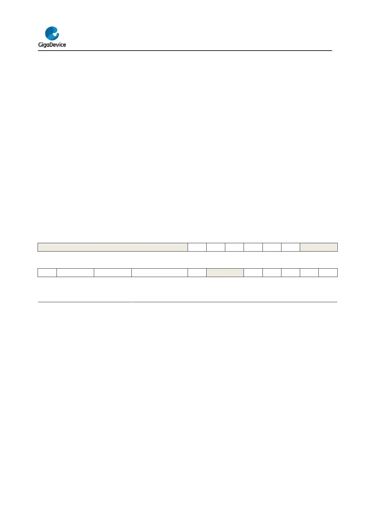
15.4.14. Tamper register (RTC_TAMP)
Address offset: 0x40
Backup domain reset: 0x0000 0000
System reset: no effect
This register has to be accessed by word (32-bit).
Must be kept at reset value.
PC15 Mode
0: No effect
1: Force PC15 to push-pull output if LXTAL is disable
PC15 Value
Only valid when LXTAL is disabled and PC15MDE = 1, PC15 output this bit data.
PC14 Mode
0: No effect
1: Force PC14 to push-pull output if LXTAL is disable
PC14 Value
Only valid when LXTAL is disabled and PC14MDE = 1, PC14 output this bit data.
PC13 Mode
0: No effect
1: Force PC13 to push-pull output if all RTC alternate functions are disabled.
PC13 value or alarm output type value


 To Next Page