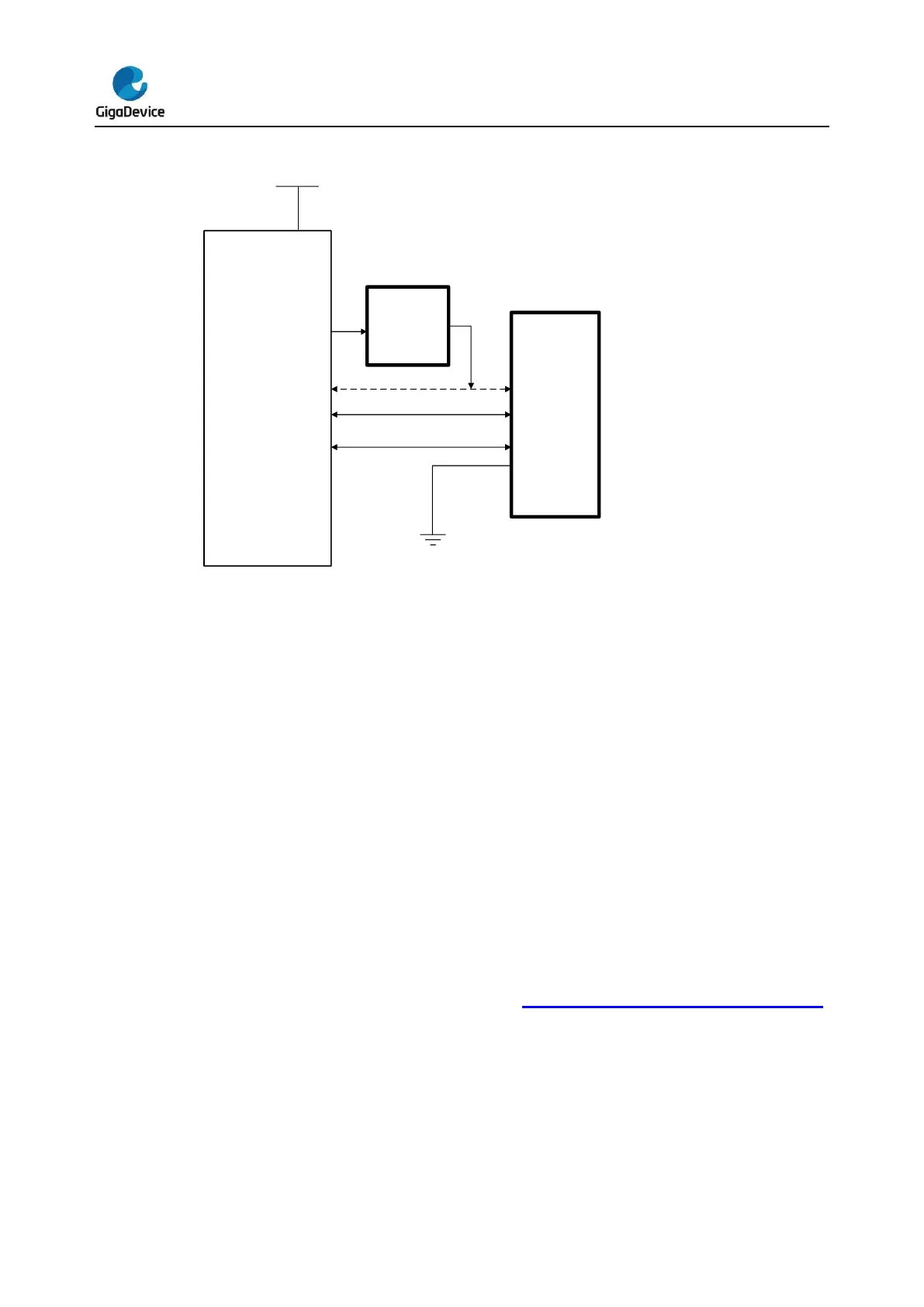
When USBFS works in host mode (FHM bit is set and FDM bit is cleared), the VBUS is 5V
power detecting pin used for voltage detection defined in USB protocol. The internal PHY
cannot supply 5V VBUS power and only has some voltage comparers, charge and
dis-charge circuits on VBUS line. So if application needs VBUS power, an external power
supply IC is needed. The VBUS connection between USBFS and the USB connector can be
omitted in host mode, so USBFS doesn’t detect the voltage level on VBUS pin and always
assumes that the 5V power is present.
When USBFS works in device mode (FHM bit is cleared and FDM bit is set), the VBUS
detection circuit is controlled by VBUSIG bit in USBFS_GCCFG register. So if the application
needn’t detect the voltage on VBUS pin, the VBUS pin can be freed for other use by setting
the VBUSIG bit, the power supply is considered always on and the pull-up resistor on DP line
is always switch on. Otherwise, the VBUS connection cannot be omitted, and USBFS
continuously monitor the VBUS voltage and will immediately switch off the pull-up resistor on
DP line once that the VBUS voltage falls below the needed valid value. This will cause a
disconnection.
The OTG mode connection is described in the Figure 23-3. Connection with OTG mode.
When USBFS works in OTG mode, the FHM, FDM bits in USBFS_GUSBCS and VBUSIG bit
in USBFS_GCCFG should be cleared. In this mode, the USBFS needs all the four pins: DM,
DP, VBUS and ID, and needs to use several voltage comparers to monitor the voltage on
these pins. USBFS also contains VBUS charge and discharge circuits to perform SRP
request described in OTG protocol. The OTG A-device or B-device is decided by the level of
ID pins. USBFS controls the pull-up or pull-down resistor during performing the HNP
protocol.


 To Next Page