GD32F3x0 User Manual
573
diagram of Sample pin and Channel Pin, i.e. PIN0 is channel pin and PIN1 is sample pin.
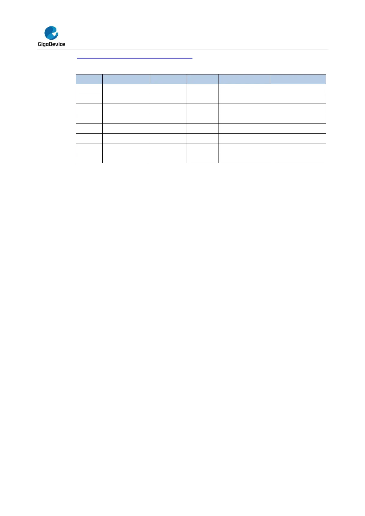
Table 22-1. Pin and analog switch state in a charge-transfer sequence
1. Discharge
Both C
x
and C
s
are discharged by closing ASW_0 and ASW_1 and configuring PIN1 to
pull down. This step is the initial operation for a correct charge transfer sequence and is
performed by software before starting a charge transfer sequence. Discharging time in this
step should be guaranteed to ensure that the voltage of C
x
and C
s
are discharged to zero.
2. Buffer Time1
Buffer time with ASW_0 and ASW_1 open, PIN0 is configured to input floating.
3. Charge
Channel pin PIN0 is configured to output high, in order to charge C
x
. ASW_0 and ASW_1
remain open during this step. The charging time should be configured (see Register Section
for detail) to ensure that the voltage of C
x
is charged to V
DD
.
4. Extend Charge
This is an optional step in a charge-transfer sequence and the behavior of all pins and
analog switches in this step is the same as Step 3. The only difference between this and step
3 is the duration time, which is configurable in TSI registers. The duration of this step
changes in each loop of a charge-transfer sequence, spreading the spectrum.
5. Buffer Time2
Buffer time with ASW_0 and ASW_1 open, PIN0 is configured to input floating.
6. Charge transfer
ASW_0 and ASW_1 are closed and PIN0 is configured to input floating to transfer charge
from C
x
to C
s
. The transfer time should be configured (see Register Section for detail) to
ensure the full transfer after that the voltage of C
x
and C
s
will be equal.
 Loading...

