application.
Slave in hardware NSS mode: NSS input, as a chip select
signal for slave.
Quad-SPI configuration
SPI is in single wire mode by default and enters into Quad-SPI mode after QMOD bit in
SPI_QCTL register is set (only available in SPI1). Quad-SPI mode can only work in master
mode.
The IO2 and IO3 pins can be driven high in normal Non-Quad-SPI mode by configuring
IO23_DRV bit in SPI_QCTL register.
The SPI is connected to external devices through 6 pins in Quad-SPI mode:
Table 20-2. Quad-SPI signal description
Transmission/Reception data 0
Transmission/Reception data 1
Transmission/Reception data 2
Transmission/Reception data 3
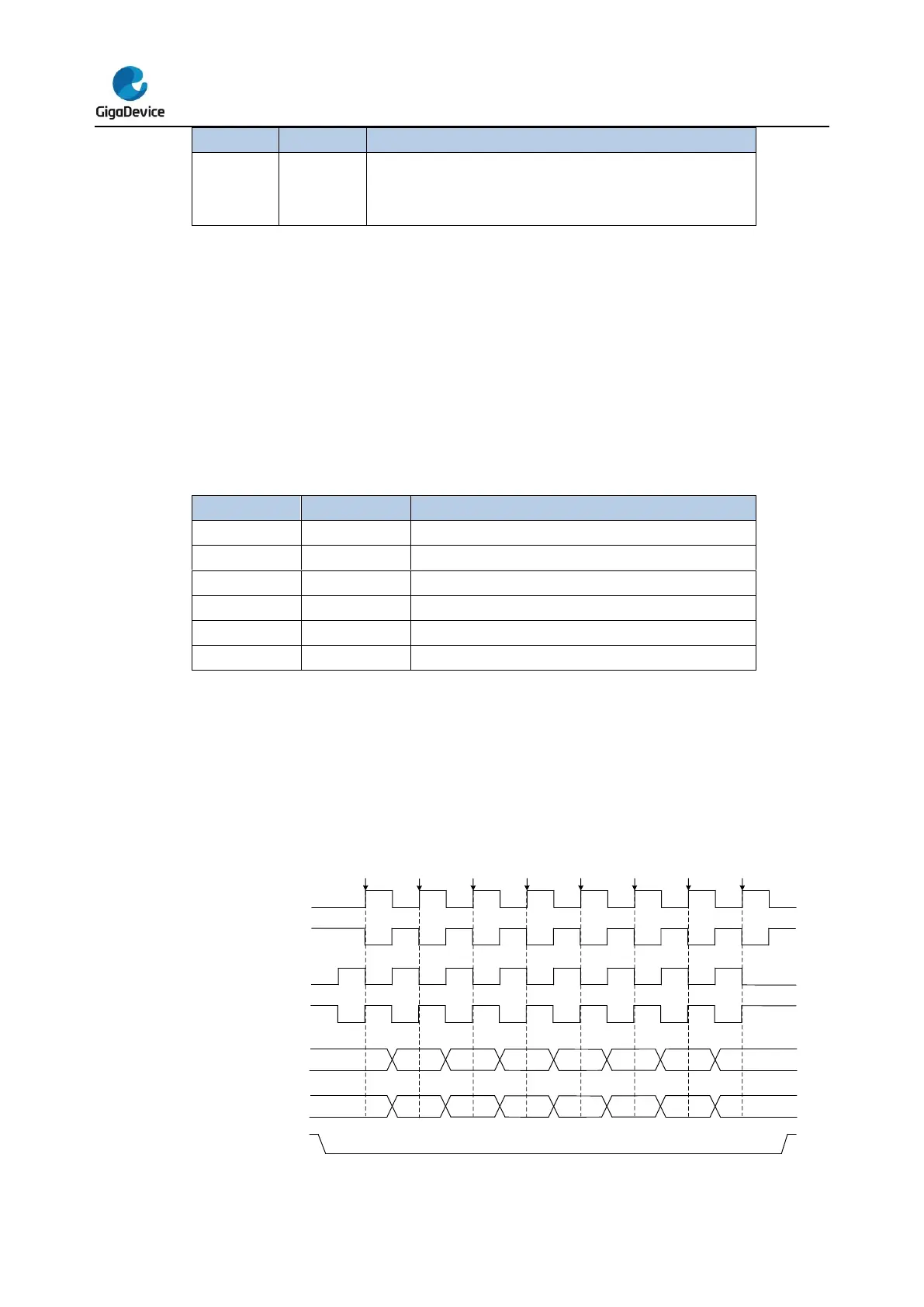
20.3.3. SPI clock timing and data format
CKPL and CKPH bits in SPI_CTL0 register decide the timing of SPI clock and data signal.
The CKPL bit decides the SCK level when SPI is in idle state and CKPH bit decides either
first or second clock edge is a valid sampling edge. These bits take no effect in TI mode.
Figure 20-2. SPI timing diagram in normal mode
SCK (CKPH=0 CKPL=0)
SCK (CKPH=0 CKPL=1)
SCK (CKPH=1 CKPL=0)
SCK (CKPH=1 CKPL=1)
LF=1
FF16=0
MOSI
MISO
NSS
D[0]
D[1]
D[2]
D[3]
D[4]
D[5]
D[6]
D[7]
sample
D[0]
D[1]
D[2]
D[3] D[4]
D[5]
D[6]
D[7]
 Loading...

