EasyManua.ls Logo

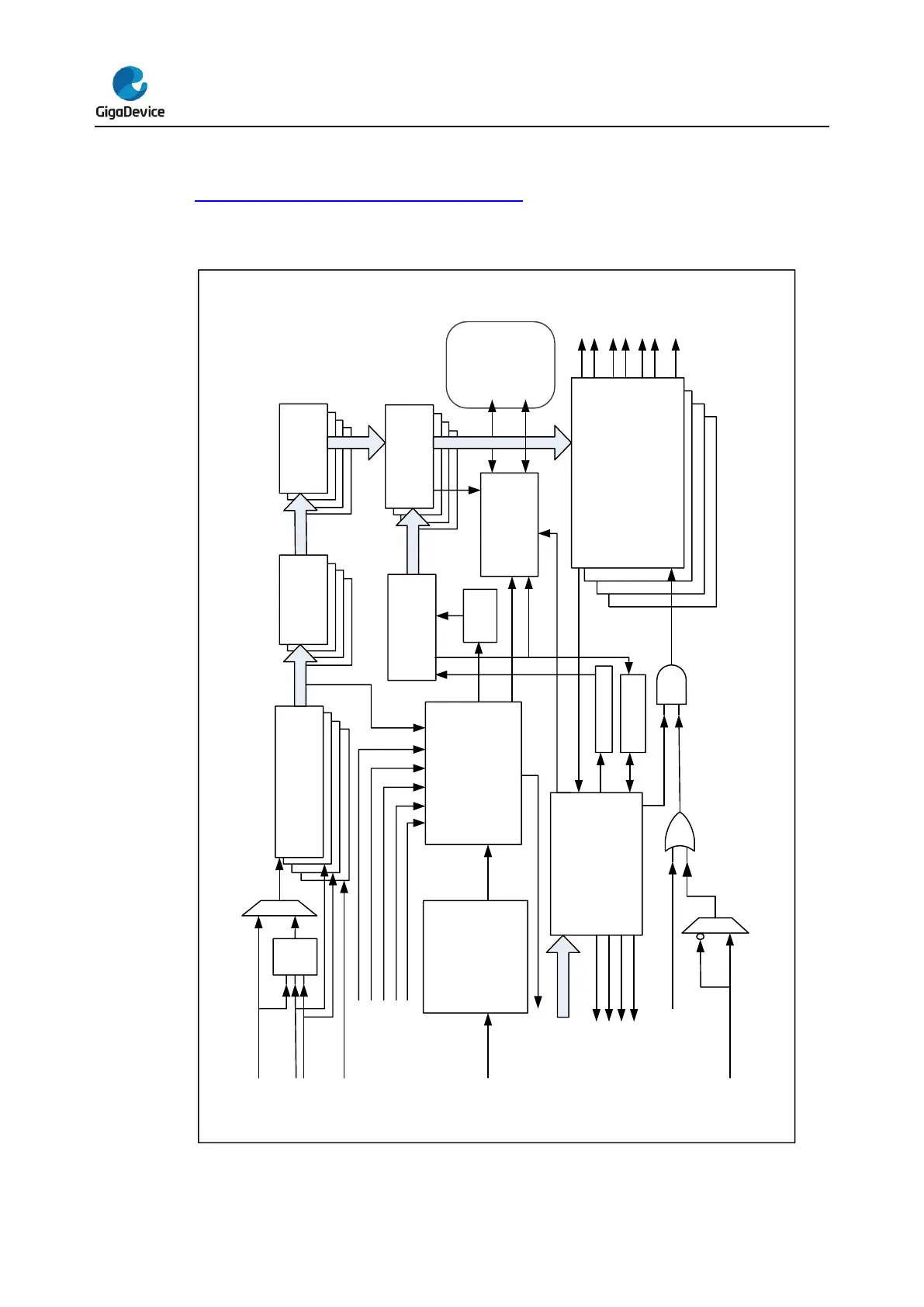
GigaDevice Semiconductor GD32F3x0 - Block Diagram; Figure 16-1. Advanced Timer Block Diagram

Default Icon
665 pages
Print Icon
To Next Page IconTo Next Page
To Previous Page IconTo Previous Page
Loading...
GD32F3x0 User Manual
252
16.1.3. Block diagram
Figure 16-1. Advanced timer block diagram provides details of the internal configuration
of the advanced timer.
Figure 16-1. Advanced timer block diagram
=1
0
0
0
0
Input Logic
Synchronizer
&Filter
&Edge Detector
Edge selector
Prescaler
Trigger processor
Trigger Selector
&Counter
Quadrate Decoder
Counter
External Trigger
Input logic
Polarity selection
Edge detector
Prescaler
Filter
TIMERx
_CHxCV
Register
/Interrupt
Register set and update
Interrupt collector and
controller
APB BUS
CK_TIMER
CH0_IN
CH1_IN
CH2_IN
CH3_IN
CI0
ITI0
ITI1
ITI2
ITI3
ETI
CAR
Repeater
Output Logic
generation of outputs signals in
compare
, PWM,and mixed modes
according to
initialization
,
complementary mode
, software
output control
, deadtime insertion
,
break input
, output mask
, and
polarity control
BRKEN
BRKIN
CKM
clock monitor
CH0_O
CH0_ON
DMA controller
TIMERx_TRGO
DMA REQ
/ACK
TIMERx_CH0
TIMERx_CH1
TIMERx_CH2
TIMERx_CH3
TIMERx_TG
TIMERx_UP
TIMERx_CMT
.
Interrupt
break
update
trig/ctrl
cap/com
CH1_O
CH1_ON
CH2_O
CH2_ON
CH3_O
req en/direct req set
PSC
PSC_CLK
TIMER_CK
ETIFP

Table of Contents