Output PWM function
In the output PWM mode (by setting the CHxCOMCTL bits to 3’b110 (PWM mode0) or to 3’b
111(PWM mode1), the channel can generate PWM waveform according to the
TIMERx_CAR registers and TIMERx_CHxCV registers.
The period is determined by TIMERx_CAR and duty cycle is determined by TIMERx_CHxCV.
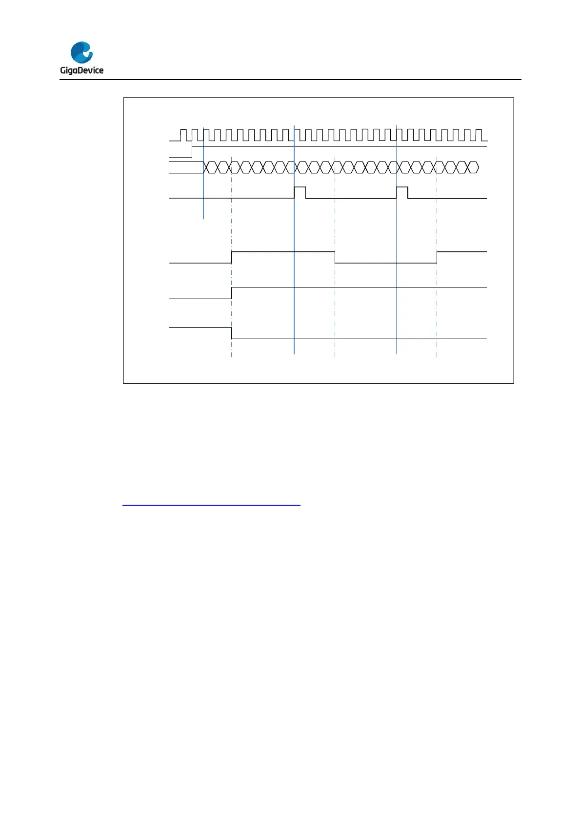
Figure 16-61. PWM mode timechart shows the PWM output mode and interrupts
waveform.
If TIMERx_CHxCV is greater than TIMERx_CAR, the output will be always active under
PWM mode0 (CHxCOMCTL==3’b110).
And if TIMERx_CHxCV is equal to zero, the output will be always inactive under PWM
mode0 (CHxCOMCTL==3’b110).
 Loading...

