GD32F3x0 User Manual
448
18.3. Function overview
The interface is externally connected to another device by the main pins listed in Table 18-1.
Description of USART important pins.
Table 18-1. Description of USART important pins
Output I/O
(single-wire/smartcard mode)
Transmit Data. High level when enabled but
nothing to be transmitted
Serial clock for synchronous communication
Clear to send in hardware flow control mode
Request to send in hardware flow control mode
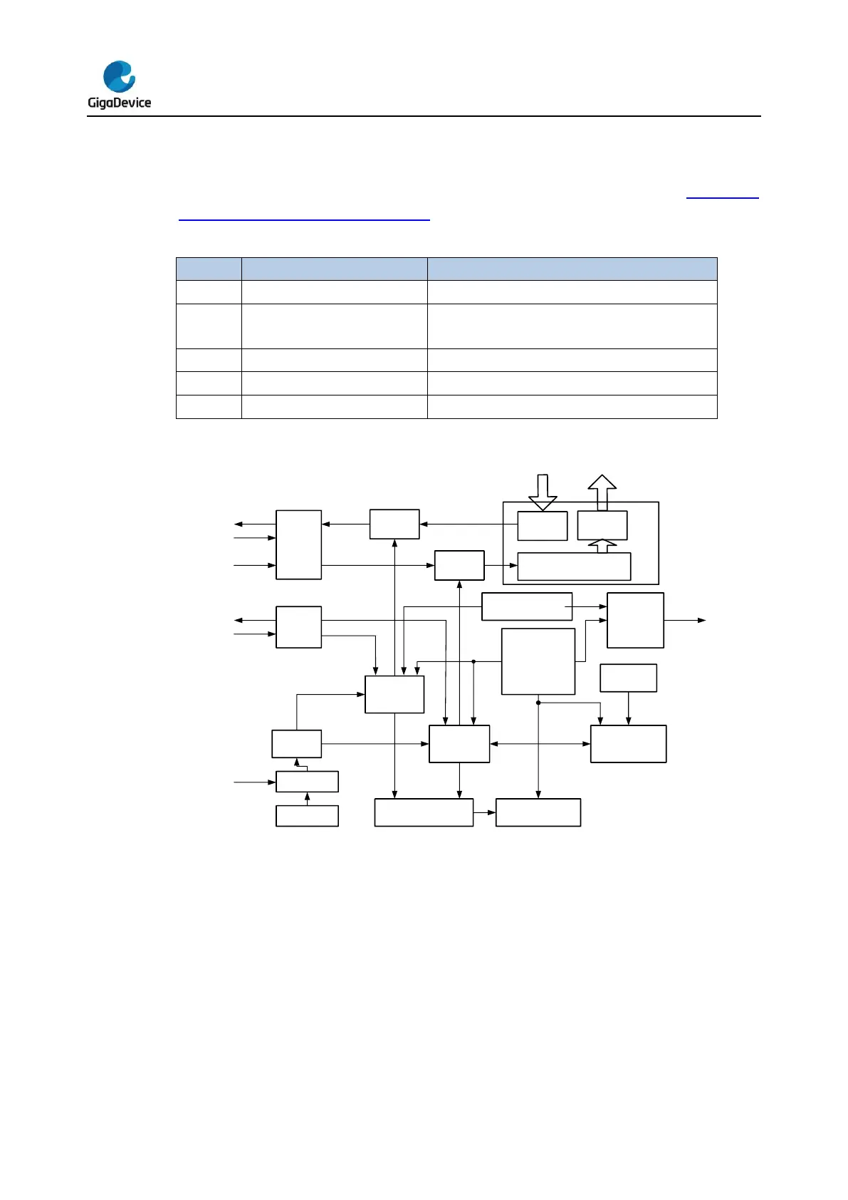
Figure 18-1. USART module block diagram
CPU/DMA
RW
IrDA
Block
TX
SW_RX
RX
CK Controler
Transmit
Shift
Register
Receive
Shift
Register
USART Control
Registers
CK
Transimit
Controler
Hardware
Flow
Controler
nRTS
nCTS
Receiver
Controler
USART
Address
Wakeup Unit
USART Guard Time
and Prescaler Register
USART Status Register
USART Interrupt
Controler
/USARTDIV
/8*(2-
OVSMOD)
USART Baud
Rate Register
UCLK
Transmitter
clock
Receiver
clock
Write
Buffer
Read
Buffer
Read FIFO
18.3.1. USART frame format
The USART frame starts with a start bit and ends up with a number of stop bits. The length of
the data frame is configured by the WL bit in the USART_CTL0 register. The last data bit can
be used as parity check bit by setting the PCEN bit of in USART_CTL0 register. When the
WL bit is reset, the parity bit is the 7th bit. When the WL bit is set, the parity bit is the 8th bit.
The method of calculating the parity bit is selected by the PM bit in USART_CTL0 register.
 Loading...

