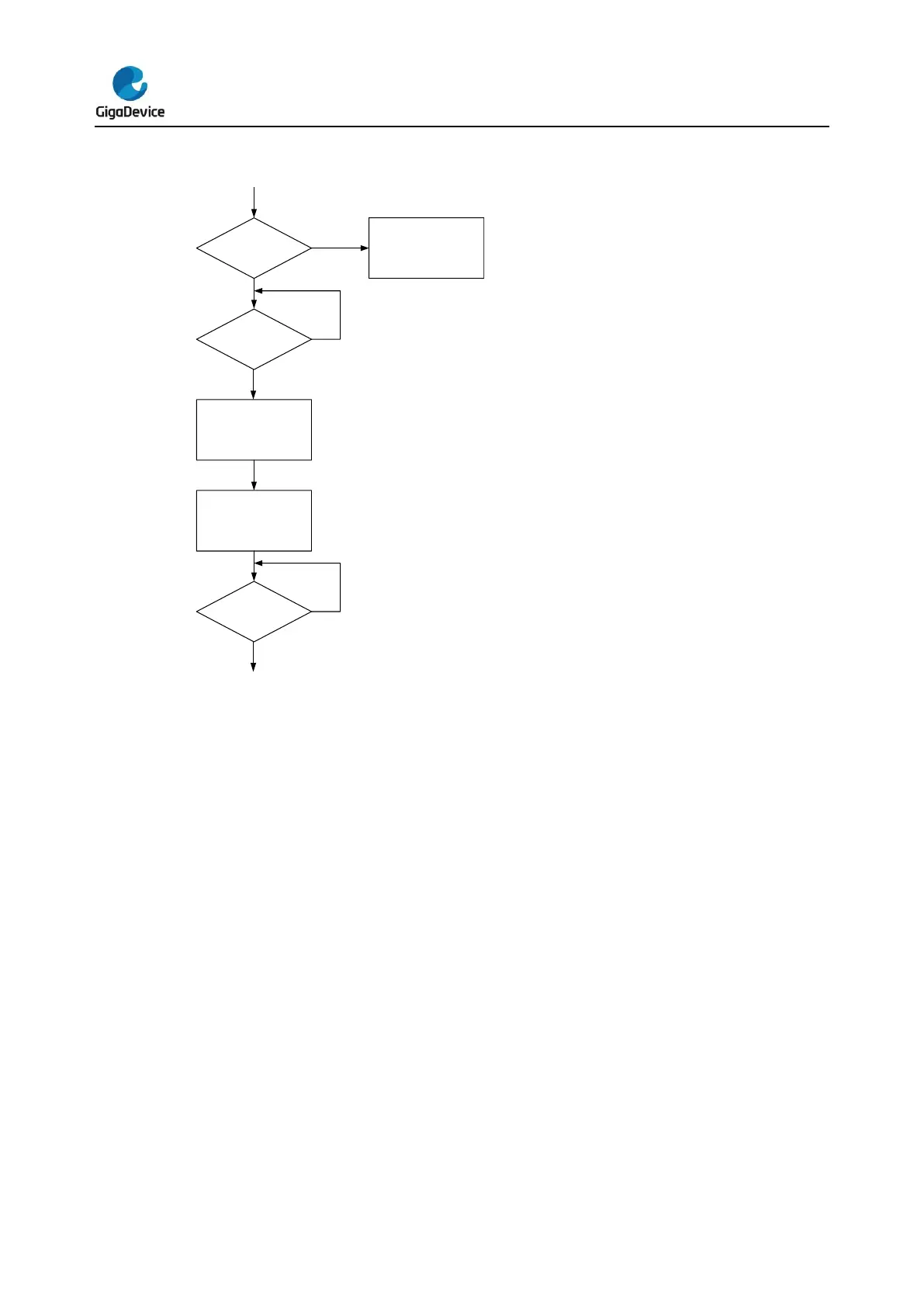
2.3.7. Option byte erase
The FMC provides an erase function which is used for initializing the option byte block in
flash. The following steps show the erase sequence.
1. Unlock the FMC_CTL register if necessary.
2. Unlock the OBWEN bit in FMC_CTL register if necessary.
3. Check the BUSY bit in FMC_STAT register to confirm that no flash memory operation is
in progress (BUSY equal to 0). Otherwise, wait until the operation has been finished.
4. Write the option byte erase command into OBER bit in FMC_CTL register.
5. Send the option byte erase command to the FMC by setting the START bit in FMC_CTL
register.
6. Wait until all the operations have been completed by checking the value of the BUSY bit
in FMC_STAT register.
7. Read and verify the flash memory by using a DBUS access if necessary.
When the operation is executed successfully, an interrupt will be triggered by FMC if the
ENDIE bit in the FMC_CTL register is set, and the ENDF in FMC_STAT register is set. The
end of this operation is indicated by the ENDF bit in the FMC_STAT register.