EasyManua.ls Logo

GigaDevice Semiconductor GD32F3x0 - Memory Map

Default Icon
665 pages
Print Icon
To Next Page IconTo Next Page
To Previous Page IconTo Previous Page
Loading...
GD32F3x0 User Manual
25
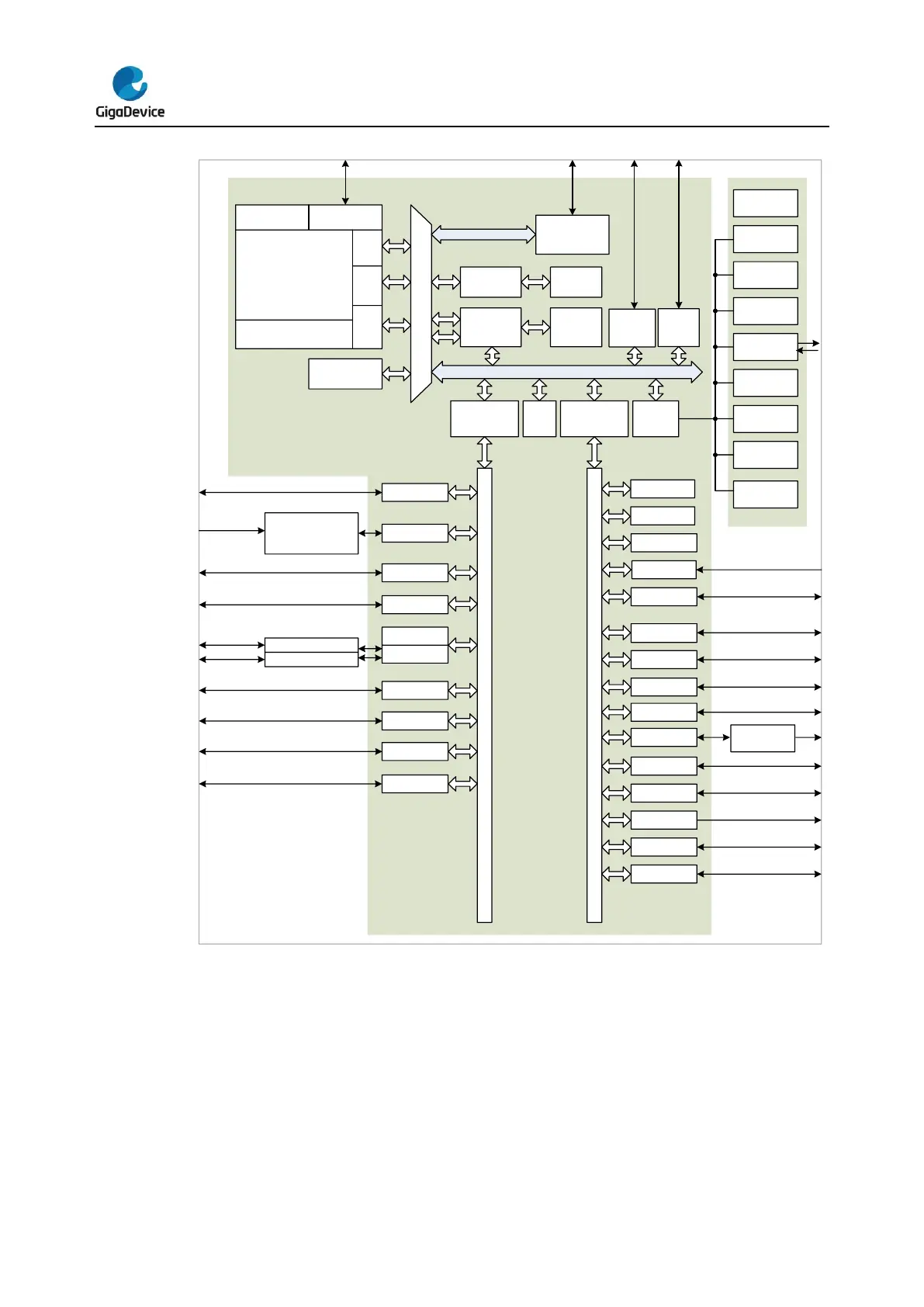
Figure 1-2. Series system architecture of GD32F3x0 series
ICode
DCode
System
NVIC
TPIU SW
Flash
Memory
Controller
Flash
Memory
AHB Matrix
SRAM
Controller
SRAM
AHB to APB
Bridge 2
GP DMA
7chs
USART0
SPI0/I2S0
ADC
TIMER16
12-bit
SAR ADC
IBus
ARM Cortex-M4
Processor
Fmax: 108MHz
POR/PDR
PLL
Fmax: 108MHz
LDO
1.2V
IRC8M
8MHz
HXTAL
4-32MHz
LVD
EXTI
TIMER0
AHB1: Fmax = 108MHz
AHB to APB
Bridge 1
CRC
RST/CLK
Controller
DBus
USBFS
AHB2: Fmax = 108MHz
GPIO Ports
A, B, C, D, F
IRC28M
28MHz
CMP
SYS Config
TIMER14
TIMER15
APB2: F
max
= 54MHz
IRC48M
48MHz
Powered by LDO (1.2V)
CMP0
CMP1
TIMER1
WWDGT
APB1: F
max
= 54MHz
TIMER5
SPI1
CTC
I2C0
RTC
FWDGT
HDMI-CEC
PMU
DAC
I2C1
12-bit
DAC
TIMER13
TIMER2
Powered by VDD/VDDA
IRC40K
40KHz
Touch
Sensing
Interface
USART1
1.3. Memory map
The Arm
®
Cortex
®
-M4 processor is structured in Harvard architecture which can use
separate buses to fetch instructions and load/store data. The instruction code and data are
both located in the same memory address space but in different address ranges. Program
memory, data memory, registers and I / O ports are organized within the same linear
4-Gbyte address space which is the maximum address range of the Cortex
®
-M4 since it has
a 32-bit bus address width. Additionally, a pre-defined memory map is provided by the

Table of Contents