GD32F3x0 User Manual
206
13.4. CMP registers
CMP base address:0x4001 001C
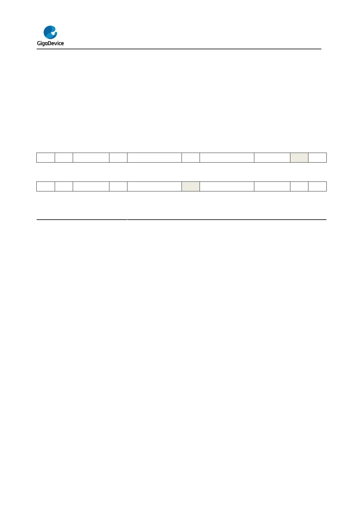
13.4.1. Control/status register (CMP_CS)
Address offset: 0x00
Reset value: 0x0000 0000
This register has to be accessed by word (32-bit).
CMP1 lock
This bit allows to have all control bits of CMP1 as read-only. It can only be set once
by software and cleared by a system reset.
0: CMP_CS[31:16] bits are read-write
1: CMP_CS[31:16] bits are read-only
CMP1 output
This bit is a copy of CMP1 output state, which is read only.
0: Non-inverting input below inverting input and the output is low
1: Non-inverting input above inverting input and the output is high
CMP1 hysteresis
These bits are used to control the hysteresis level.
00: No hysteresis
01: Low hysteresis
10: Medium hysteresis
11: High hysteresis
Polarity of CMP1 output
This bit is used to select the polarity of CMP1 output.
0: Output is not inverted
1: Output is inverted
CMP1 output selection
These bits are used to select the destination of the CMP1 output.
000: No selection
001: TIMER0 break input


 To Next Page