18.3.10. IrDA SIR ENDEC mode
The IrDA mode is enabled by setting the IREN bit in USART_CTL2. The LMEN, STB[1:0],
CKEN bits in USART_CTL1 and HDEN, SCEN bits in USART_CTL2 should be cleared in
IrDA mode.
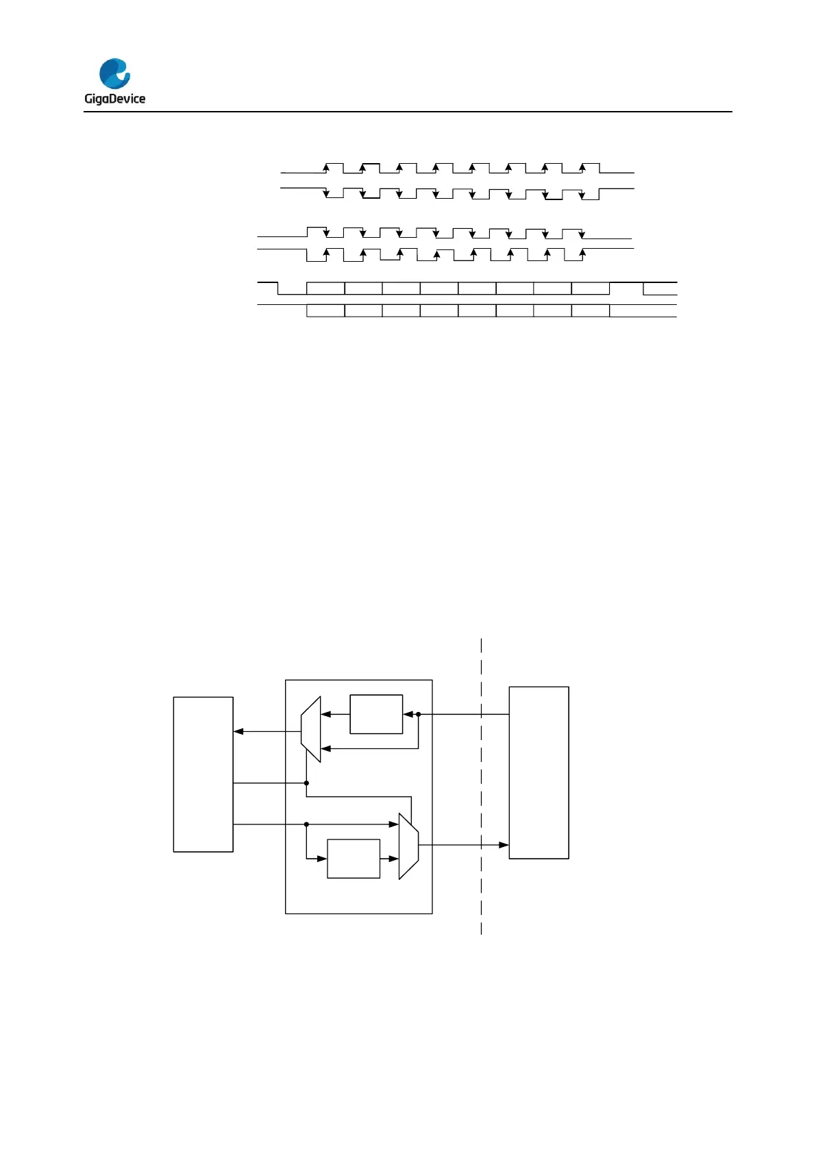
In IrDA mode, the USART transmission data frame is modulated in the SIR transmit encoder
and transmitted to the infrared LED through the TX pin. The SIR receive decoder receives
the modulated signal from the infrared LED through the RX pin, and puts the demodulated
data frame to the USART receiver. The baud rate should not be larger than 115200 for the
encoder.
Figure 18-13. IrDA SIR ENDEC module
In IrDA mode, the polarity of the TX and RX pins is different. The TX pin is usually at low
state, while the RX pin is usually at high state. The IrDA pins keep stable to represent the
logic ‘1’, while an infrared light pulse on the IrDA pins (a Return to Zero signal) represents the
logic ‘0’. The pulse width should be 3/16 of a bit period. The IrDA could not detect any pulse if
 Loading...

