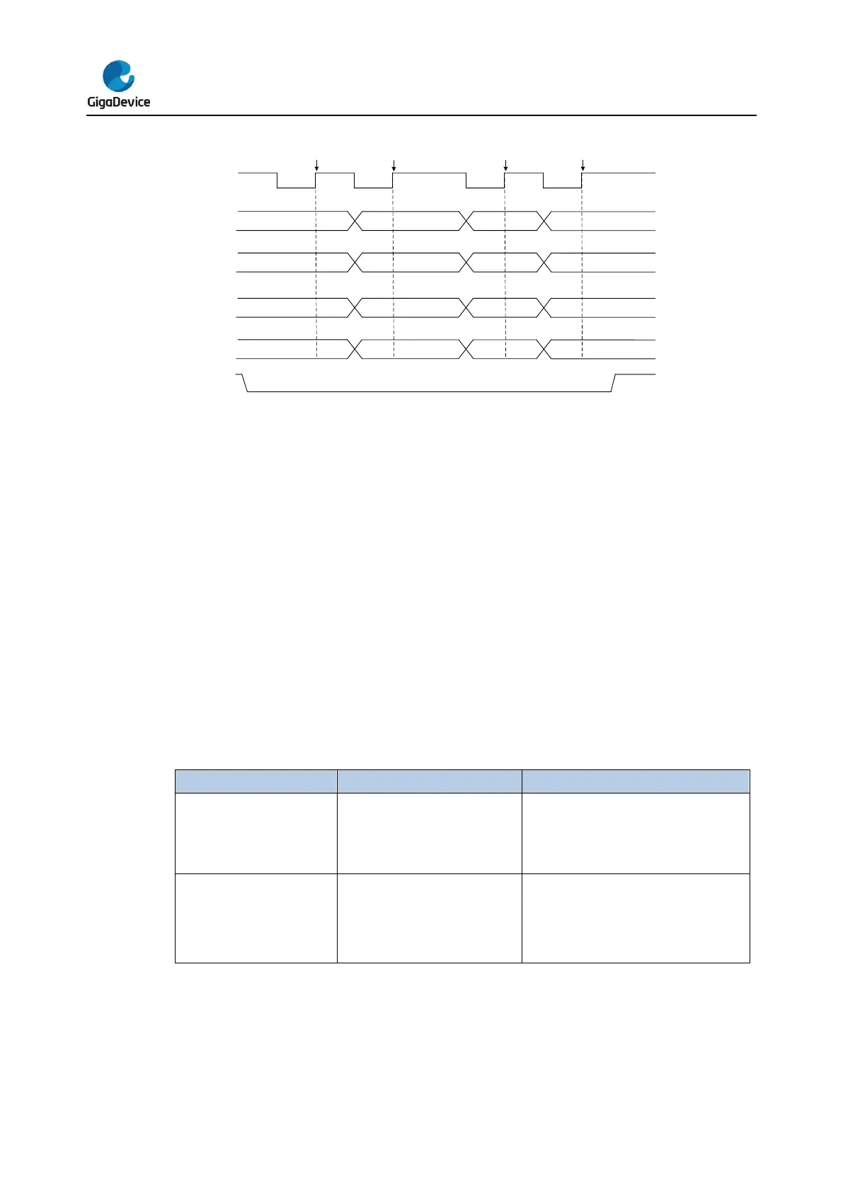
In normal mode, the length of data is configured by the FF16 bit in the SPI_CTL0 register.
Data length is 16 bits if FF16=1, otherwise is 8 bits. The data frame length is fixed to 8 bits in
Quad-SPI mode.
Data order is configured by LF bit in SPI_CTL0 register, and SPI will send the LSB first if
LF=1, or the MSB if LF=0. The data order is fixed to MSB first in TI mode.
20.3.4. NSS function
Slave mode
When slave mode is configured (MSTMOD=0), SPI gets NSS level from NSS pin in
hardware NSS mode (SWNSSEN = 0) or from SWNSS bit in software NSS mode
(SWNSSEN = 1) and transmits/receives data only when NSS level is low. In software NSS
mode, NSS pin is not used.
Table 20-3. NSS function in slave mode
SPI slave NSS level is determined by
the SWNSS bit.
SWNSS = 0: NSS level is low
SWNSS = 1: NSS level is high
Master mode
In master mode (MSTMOD=1) if the application uses multi-master connection, NSS can be
configured to hardware input mode (SWNSSEN=0, NSSDRV=0) or software mode
(SWNSSEN=1). Then, once the NSS pin (in hardware NSS mode) or the SWNSS bit (in


 To Next Page