GD32F3x0 User Manual
29
register 2 (SYSCFG_CFG2). The error flag can be connected to the break input of TIMER 0/
TIMER 14/ TIMER 15/ TIMER 16, if the SRAM_PARITY_ERROR_LOCK control bit in the
system configuration register 2 (SYSCFG_CFG2) is set to 1.
The real data width of the SRAM is 36 bits, including 32 bits for data and 4 bits for parity (1
bit per byte). When writing, the parity bits are computed and stored into the SRAM. When
reading, the parity bits are also computed using the stored data in SRAM. The computed
parity bits are compared with the stored parity bits which are computed during the writing
access. If they are different, the parity check fails.
Note: Enabling the SRAM parity check, it is recommended to initialize the whole SRAM
memory by software at the beginning of the code, in order to avoid getting parity check errors
when reading non-initialized locations.
1.3.3. On-chip Flash memory
The devices provide up to 128 KB of on-chip flash memory. The flash memory consists of up
to 128 KB main flash organized into 128 pages with 1 KB capacity per page and a 3 KB
information block for the boot loader. The following table shows details.
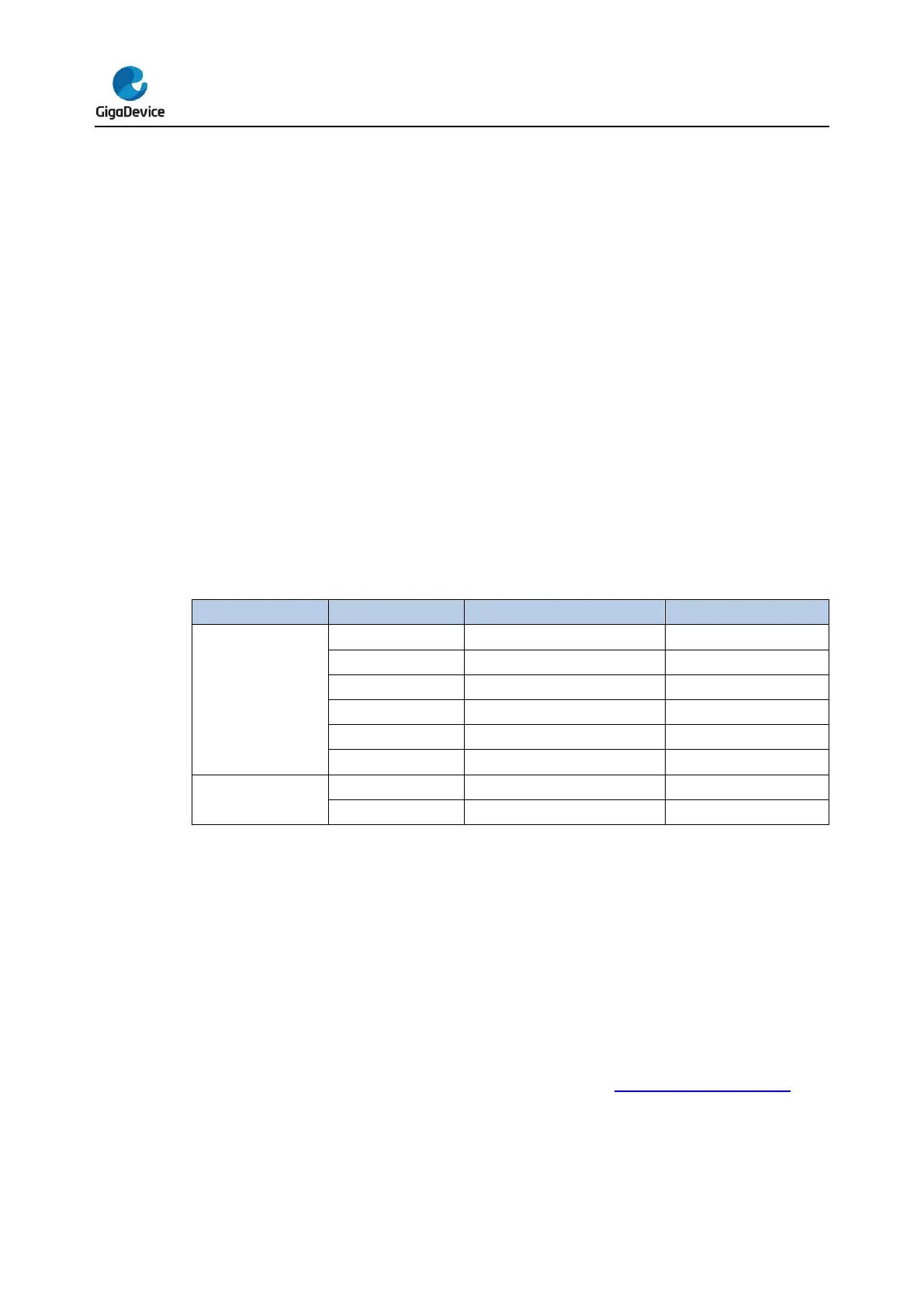
Table 1-2. Flash module organization
Read accesses to the preceding 64 pages can be performed 32 bits per cycle without any
wait state. All of byte, half-word (16 bits) and word (32 bits) read accesses are supported.
The flash memory can be programmed half-word (16 bits) or word (32 bits) at a time. Each
page of the flash memory can be erased individually. The whole flash memory space except
information blocks can be erased at a time.
1.4. Boot configuration
The GD32F3x0 series provide three kinds of boot sources which can be selected using the
bit BOOT1_n in the user option byte (refer to Chapter 2.3.9 Option byte description) and
the BOOT0 pin. The value on the BOOT0 pin is latched on the 4th rising edge of SYSCLK
after a reset. It is up to the user to set the BOOT1_n and BOOT0 after a power-on reset or a
system reset to select the required boot source. The details are shown in the following table.