GD32F3x0 User Manual
43
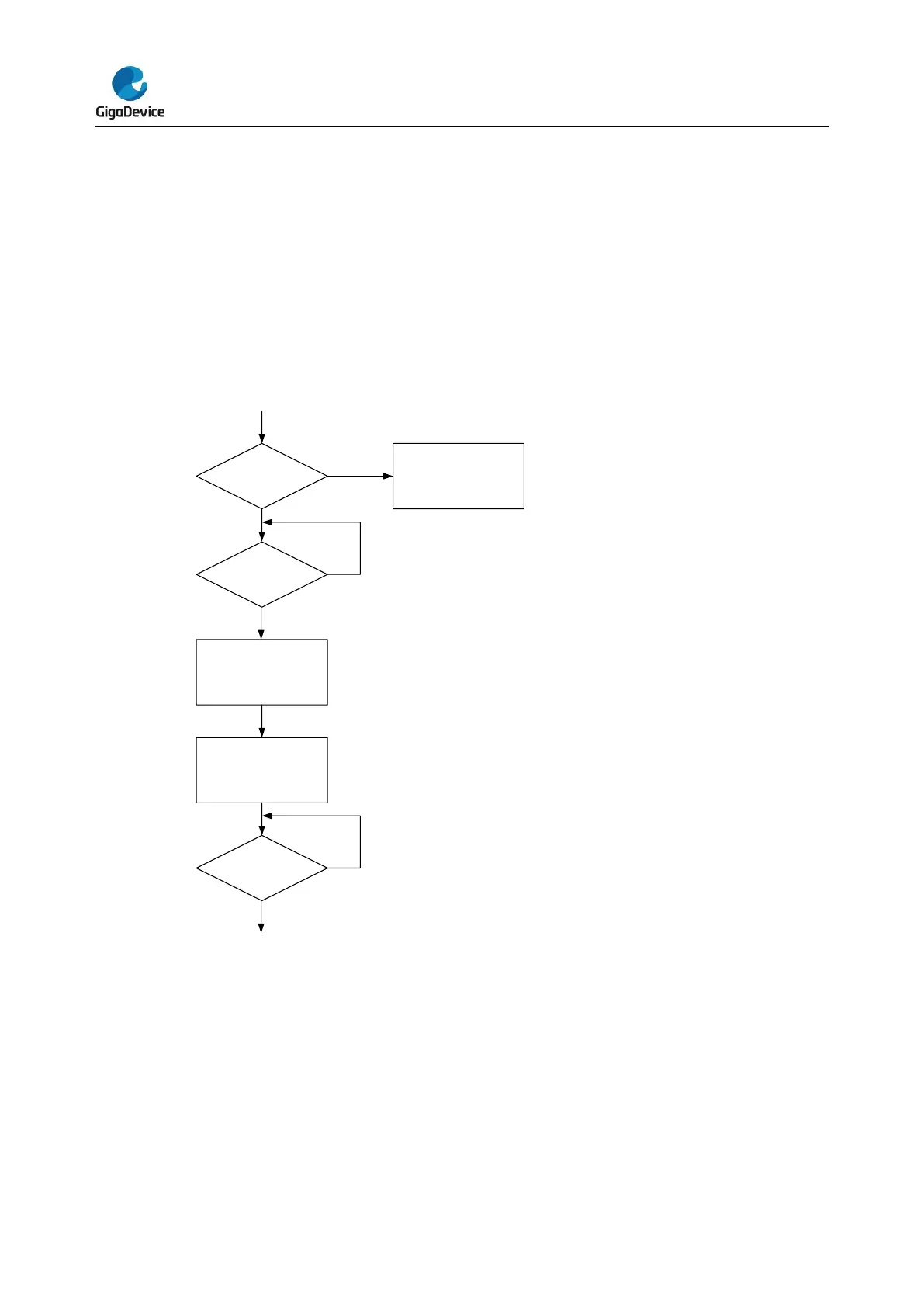
moment, if the ENDIE bit in the FMC_CTL register is set, an interrupt will be triggered by
FMC. It is notable that a correct target page address must be confirmed, otherwise the
software may run out of control if the incorrect target erase page is being used for fetching
codes or accessing data. The FMC will not provide any notification when this occurs.
Additionally, the page erase operation will be ignored on protected pages. A Flash Operation
Error interrupt will be triggered by the FMC if the ERRIE bit in the FMC_CTL register is set.
The software can check the WPERR bit in the FMC_STAT register to detect this condition in
the interrupt handler. The end of this operation is indicated by the ENDF bit in the
FMC_STAT register. The following figure shows the page erase operation flow.
Figure 2-1. Process of page erase operation
2.3.5. Mass erase
The FMC provides a complete erase function which is used for initializing the Main Flash
Block contents. The following steps show the mass erase register access sequence.
1. Unlock the FMC_CTL register if necessary.
2. Check the BUSY bit in FMC_STAT register to confirm that no flash memory operation is
in progress (BUSY equal to 0). Otherwise, wait until the operation has been finished.
3. Write the mass erase command into MER bit in FMC_CTL register.
 Loading...

