GD32F3x0 User Manual
377
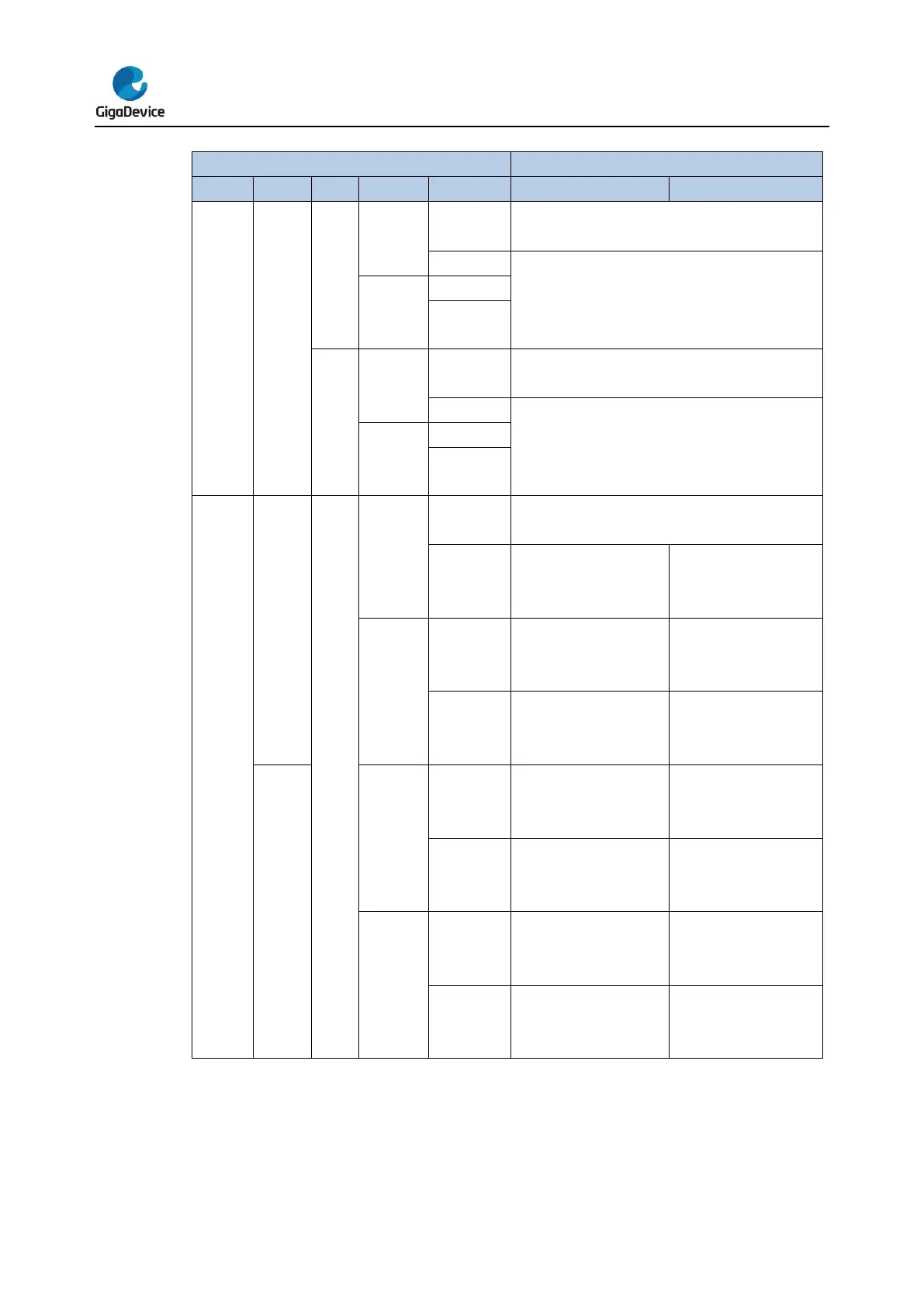
Table 16-7. Complementary outputs controlled by parameters
CHx_O / CHx_ON = LOW
CHx_O / CHx_ON output disable.
CHx_O = CHxP CHx_ON = CHxNP
CHx_O/CHx_ON output disable.
If clock is enable:
CHx_O = ISOx CHx_ON = ISOxN
CHx_O = CHxP CHx_ON = CHxNP
CHx_O/CHx_ON output disable.
CHx_O = CHxP CHx_ON = CHxNP
CHx_O/CHx_ON output enable.
If clock is enable:
CHx_O = ISOx CHx_ON = ISOxN
CHx_O/CHx_ON = LOW
CHx_O/CHx_ON output disable.
CHx_O = LOW
CHx_O output disable.
CHx_ON=OxCPRE⊕
CHxNP
CHx_ON output enable
CHx_O=OxCPRE⊕
CHxP
CHx_O output enable
CHx_ON = LOW
CHx_ON output
disable.
CHx_O=OxCPRE⊕
CHxP
CHx_O output enable
CHx_ON=(!OxCPRE)⊕
CHxNP
CHx_ON output enable
CHx_O = CHxP
CHx_O output disable.
CHx_ON = CHxNP
CHx_ON output
disable.
CHx_O = CHxP
CHx_O output enable
CHx_ON=OxCPRE⊕
CHxNP
CHx_ON output enable
CHx_O=OxCPRE⊕
CHxP
CHx_O output enable
CHx_ON = CHxNP
CHx_ON output enable.
CHx_O=OxCPRE⊕
CHxP
CHx_O output enable
CHx_ON=(!OxCPRE)⊕
CHxNP
CHx_ON output enable.
Insertion dead time for complementary PWM
The dead time insertion is enabled when both CHxEN and CHxNEN are configured to 1’b1, it
is also necessary to configure POEN to 1. The field named DTCFG defines the dead time
delay that can be used for channel 0. The detail about the delay time, refer to the register


 To Next Page