GD32F3x0 User Manual
532
than the data length, the valid data is aligned to LSB for LSB justified standard while the valid
data is aligned to MSB for MSB justified standard. The timing diagrams for the cases that the
channel length is greater than the data length are shown below.
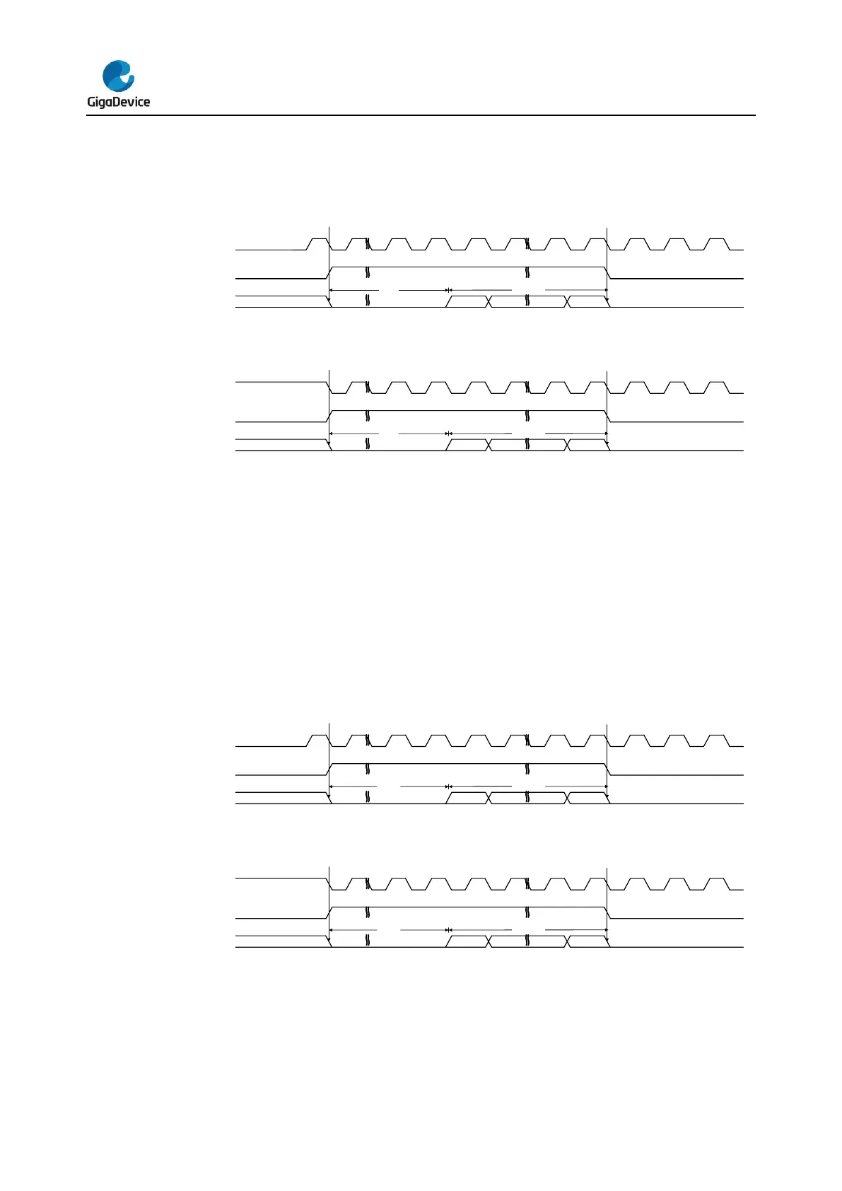
Figure 20-31. LSB justified standard timing diagram (DTLEN=01, CHLEN=1, CKPL=0)
I2S_CK
I2S_SD
8-bit 0
frame 1 (channel left) frame 2 (channel right)
I2S_WS
24-bit data
MSB LSB
Figure 20-32. LSB justified standard timing diagram (DTLEN=01, CHLEN=1, CKPL=1)
I2S_CK
I2S_SD
8-bit 0
frame 1 (channel left) frame 2 (channel right)
I2S_WS
24-bit data
MSB LSB
When the packet type is 24-bit data packed in 32-bit frame, two write or read operations to or
from the SPI_DATA register are needed to complete the transmission of a frame. In
transmission mode, if a 24-bit data D[23:0] is going to be sent, the first data written to the
SPI_DATA register should be a 16-bit data. The higher 8 bits of the 16-bit data can be any
value and the lower 8 bits should be D[23:16]. The second data written to the SPI_DATA
register should be D[15:0]. In reception mode, if a 24-bit data D[23:0] is received, the first
data read from the SPI_DATA register is a 16-bit data. The high 8 bits of this 16-bit data are
zeros and the lower 8 bits are D[23:16]. The second data read from the SPI_DATA register is
D[15:0].
Figure 20-33. LSB justified standard timing diagram (DTLEN=00, CHLEN=1, CKPL=0)
I2S_CK
I2S_SD
16-bit 0
frame 1 (channel left) frame 2 (channel right)
I2S_WS
16-bit data
MSB LSB
Figure 20-34. LSB justified standard timing diagram (DTLEN=00, CHLEN=1, CKPL=1)
I2S_CK
I2S_SD
16-bit 0
frame 1 (channel left) frame 2 (channel right)
I2S_WS
16-bit data
MSB LSB
When the packet type is 16-bit data packed in 32-bit frame, only one write or read operation
to or from the SPI_DATA register is needed to complete the transmission of a frame. The
remaining 16 bits are forced by hardware to 0x0000 to extend the data to 32-bit format.