GD32F3x0 User Manual
41
2. Flash memory controller (FMC)
2.1. Overview
The Flash Memory Controller, FMC, provides all the necessary functions for the on-chip
flash memory. There is no waiting time within 64K bytes while CPU executes instruction. It
also provides page erase, mass erase, and word / half-word / bit program for operations for
flash memory.
2.2. Characteristics
Up to 128 KB of on-chip flash memory for storing instruction and data
No waiting time within 64K bytes when CPU executes instruction
A long delay when fetch 64K ~ 128K bytes date from flash
3K bytes information block for boot loader
16 bytes option bytes block for user application requirements
1K bytes page size
Word / half-word / bit programming, page erase and mass erase operation
Flash read protection to prevent illegal code/data access
Page erase/program protection to prevent unexpected operation
2.3. Function overview
2.3.1. Flash memory architecture
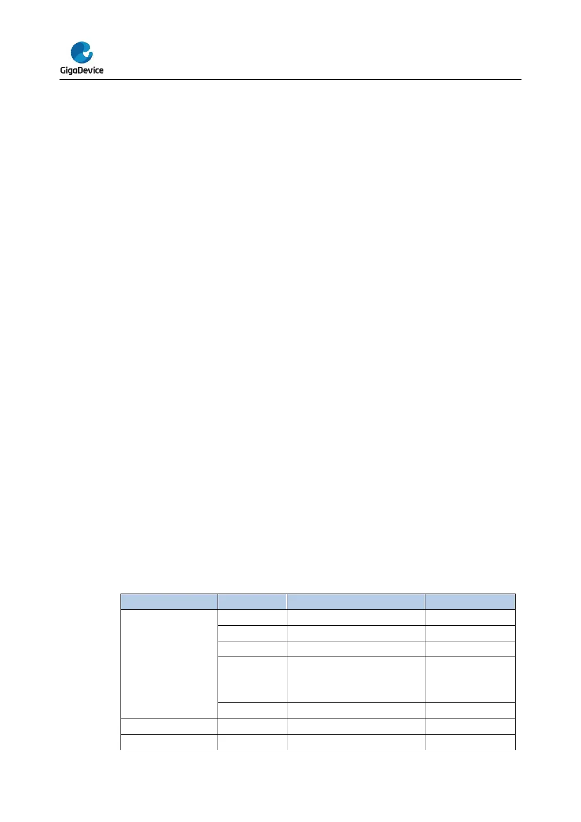
The flash memory consists of up to 128 KB main flash organized into 128 pages with 1 KB
capacity per page and a 3 KB Information Block for the Boot Loader. The main flash memory
contains a total of up to 128 pages which can be erased individually. The following table
shows the base address and size.
Table 2-1. Base address and size for flash memory