EasyManua.ls Logo

GigaDevice Semiconductor GD32F3x0 - Register Definition

Default Icon
665 pages
Print Icon
To Next Page IconTo Next Page
To Previous Page IconTo Previous Page
Loading...
GD32F3x0 User Manual
166
10.4. Register definition
DBG base address: 0xE004 2000
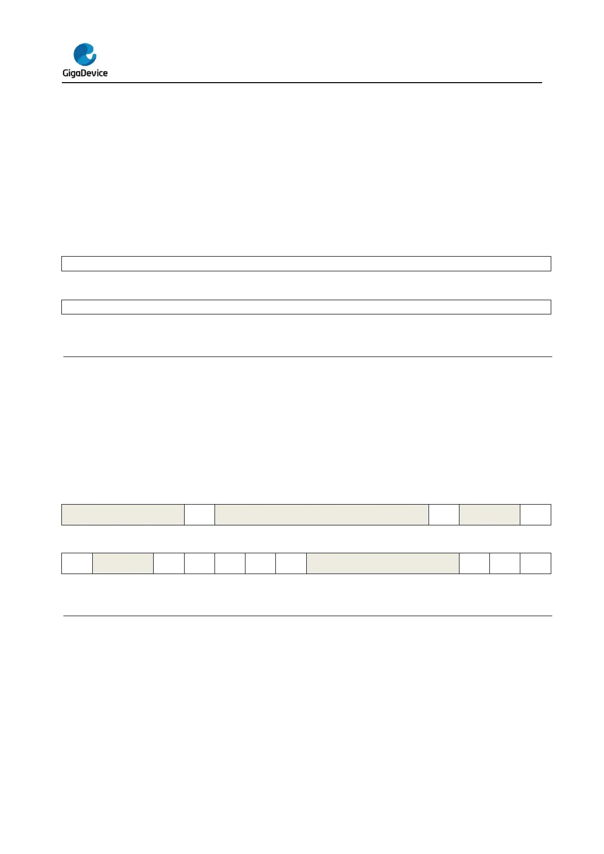
10.4.1. ID code register (DBG_ID)
Address: 0xE004 2000
Read only
This register has to be accessed by word(32-bit).
31
30
29
28
27
26
25
24
23
22
21
20
19
18
17
16
ID_CODE[31:16]
r
15
14
13
12
11
10
9
8
7
6
5
4
3
2
1
0
ID_CODE[15:0]
r
Bits
Fields
Descriptions
31:0
ID_CODE[31:0]
DBG ID code register
These bits can only be read by software. These bits are unchanged constant.
10.4.2. Control register 0 (DBG_CTL0)
Address offset: 0x04
Reset value: 0x0000 0000, power reset only
This register has to be accessed by word(32-bit).
31
30
29
28
27
26
25
24
23
22
21
20
19
18
17
16
Reserved.
TIMER13
_HOLD
Reserved
TIMER5_
HOLD
Reserved
I2C1_HO
LD
rw
rw
rw
15
14
13
12
11
10
9
8
7
6
5
4
3
2
1
0
I2C0_HO
LD
Reserved
TIMER2_
HOLD
TIMER1_
HOLD
TIMER0_
HOLD
WWDGT
_HOLD
FWDGT_
HOLD
Reserved
STB_
HOLD
DSLP_
HOLD
SLP_
HOLD
rw
rw
rw
rw
rw
rw
rw
rw
rw
Bits
Fields
Descriptions
31:28
Reserved
Must be kept at reset value.
27
TIMER13_HOLD
TIMER13 hold bit
This bit is set and reset by software
0: no effect
1: hold the TIMER13 counter for debugging when the core is halted.
26:20
Reserved
Must be kept at reset value.
19
TIMER5_HOLD
TIMER5 hold bit
This bit is set and reset by software.

Table of Contents

Related product manuals