GD32F3x0 User Manual
485
if the FMPEN bit in I2C_FMPCFG is set. Due to the variety of different technology devices
(CMOS, NMOS, bipolar) that can be connected to the I2C-bus, the voltage levels of the
logical ‘0’ (LOW) and ‘1’ (HIGH) are not fixed and depend on the associated level of V
DD
.
19.3.2. Data validation
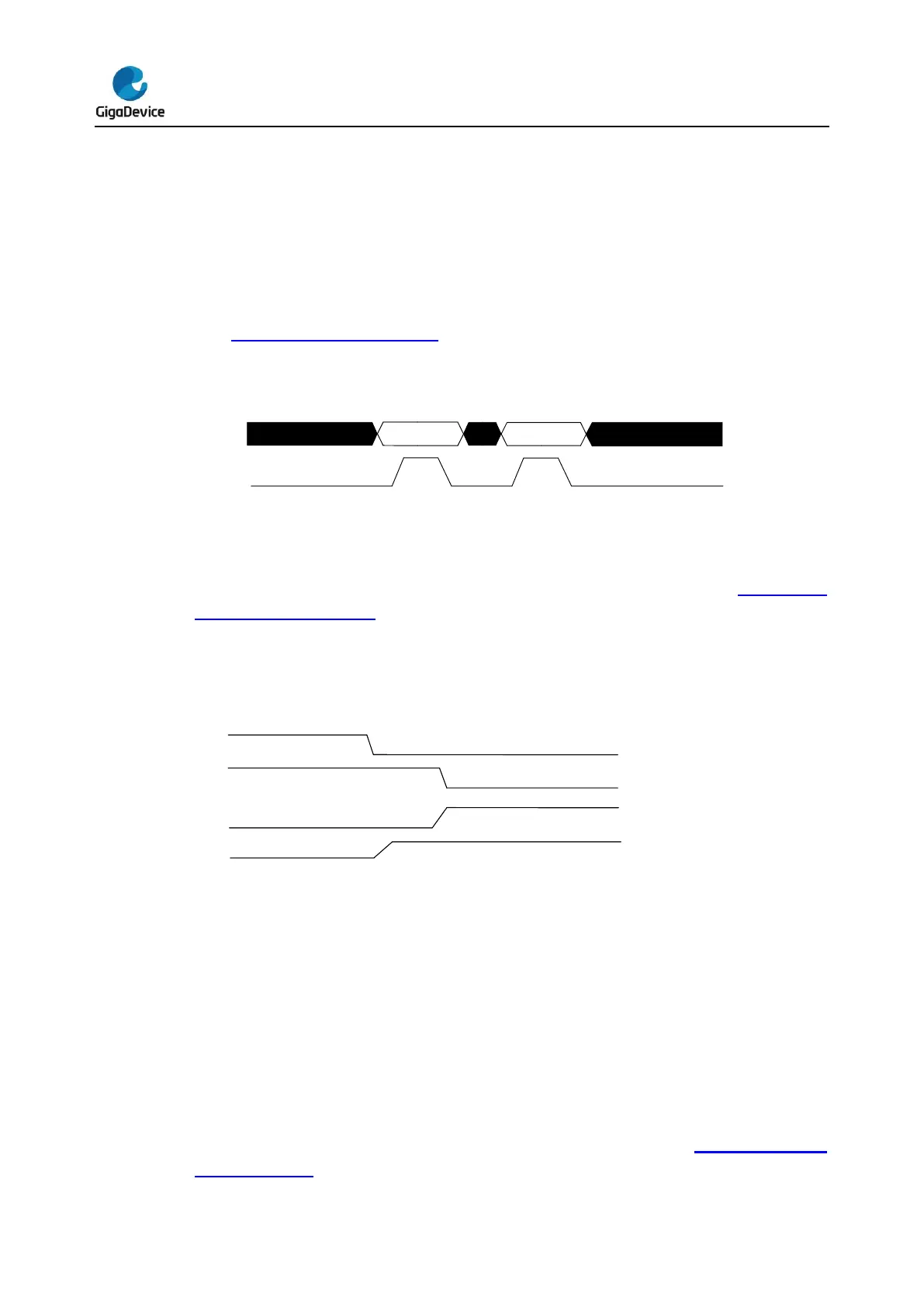
The data on the SDA line must be stable during the HIGH period of the clock. The HIGH or
LOW state of the SDA line can only change when the clock signal on the SCL line is LOW
(see Figure 19-2. Data validation). One clock pulse is generated for each data bit to be
transferred.
Figure 19-2. Data validation
19.3.3. START and STOP signal
All transmissions begin with a START and are terminated by a STOP (see Figure 19-3.
START and STOP signal). A HIGH to LOW transition on the SDA line while SCL is HIGH
defines a START signal. A LOW to HIGH transition on the SDA line while SCL is HIGH
defines a STOP signal.
Figure 19-3. START and STOP signal
19.3.4. Clock synchronization
Two masters can begin transmitting on a free bus at the same time and there must be a
method for deciding which master takes control of the bus and completes its transmission.
This is done by clock synchronization and bus arbitration. In a single master system, clock
synchronization and bus arbitration are unnecessary.
Clock synchronization is performed using the wired-AND connection of I2C interfaces to the
SCL line. This means that a HIGH to LOW transition on the SCL line causes the masters
concerned to start counting their LOW period, and once a master clock has gone LOW, it
holds the SCL line in that state until the clock HIGH state is reached (see Figure 19-4. Clock
synchronization). However, if another clock is still within its LOW period, the LOW to HIGH


 To Next Page