GD32F3x0 User Manual
536
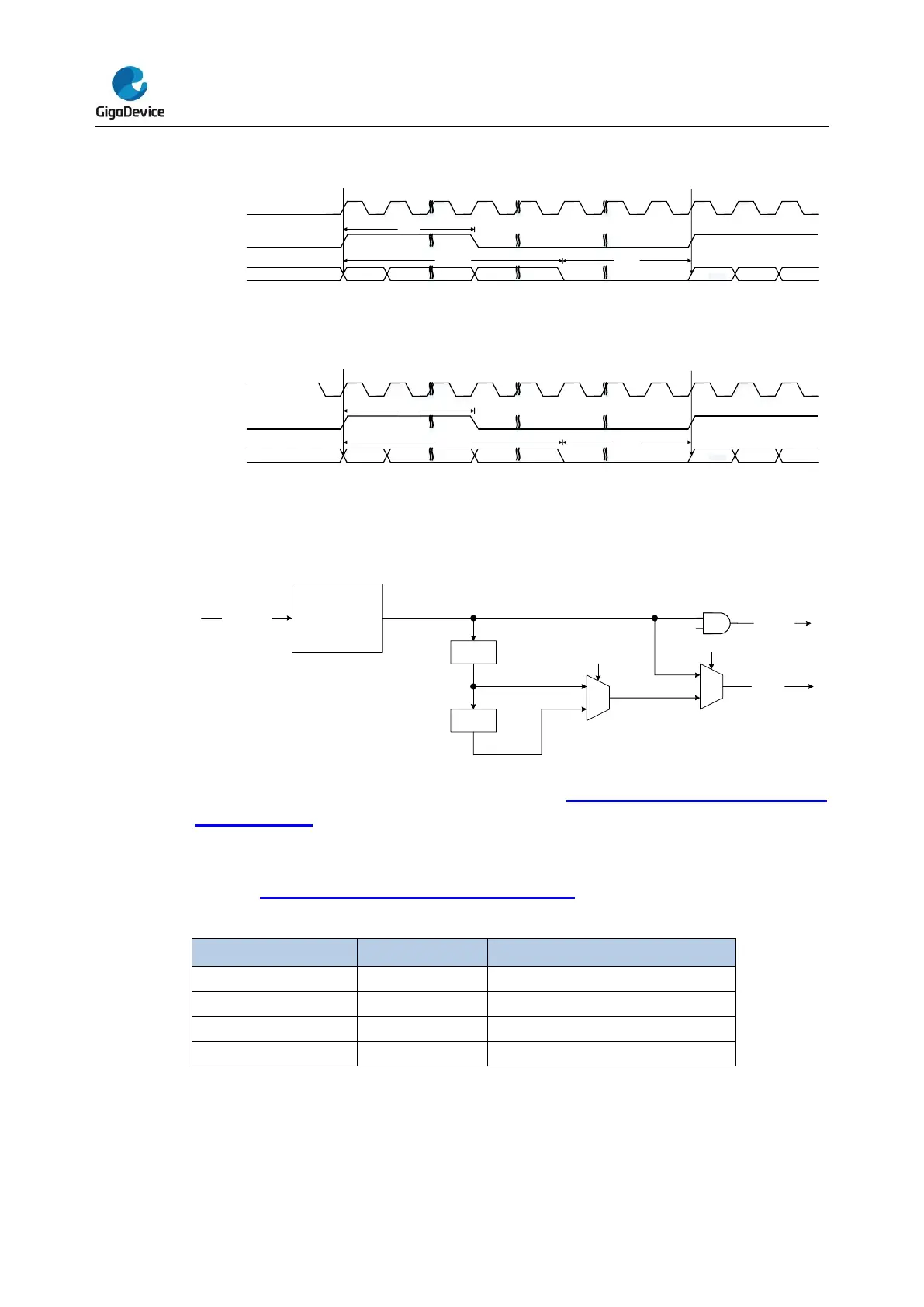
Figure 20-49. PCM standard long frame synchronization mode timing diagram
(DTLEN=00, CHLEN=1, CKPL=0)
I2S_CK
I2S_SD
16-bit data
MSB
I2S_WS
MSB
frame 1 frame 2
13 bits
16-bit 0
Figure 20-50. PCM standard long frame synchronization mode timing diagram
(DTLEN=00, CHLEN=1, CKPL=1)
I2S_CK
I2S_SD
16-bit data
MSB
I2S_WS
MSB
frame 1 frame 2
13 bits
16-bit 0
20.4.4. I2S clock
Figure 20-51. Block diagram of I2S clock generator
8-bit
Configurable
Divider
I2SCLK
Frequency dividing ratio =
DIV * 2 + OF
DIV4
DIV2
1
0
CHLEN
0
1
MCKOEN
I2S_CK
I2S_MCK
MCKOEN
The block diagram of I2S clock generator is shown as Figure 20-51. Block diagram of I2S
clock generator.The I2S interface clocks are configured by the DIV bits, the OF bit, the
MCKOEN bit in the SPI_I2SPSC register and the CHLEN bit in the SPI_I2SCTL register. The
source clock is the system clock(CK_SYS). The I2S bitrate can be calculated by the formulas
shown in Table 20-7. I2S bitrate calculation formulas.
Table 20-7. I2S bitrate calculation formulas
I2SCLK / (8 * (DIV * 2 + OF))
I2SCLK / (4 * (DIV * 2 + OF))
The relationship between audio sampling frequency (Fs) and I2S bitrate is defined by the
following formula:
Fs = I2S bitrate / (number of bits per channel * number of channels)


 To Next Page