GD32F3x0 User Manual
533
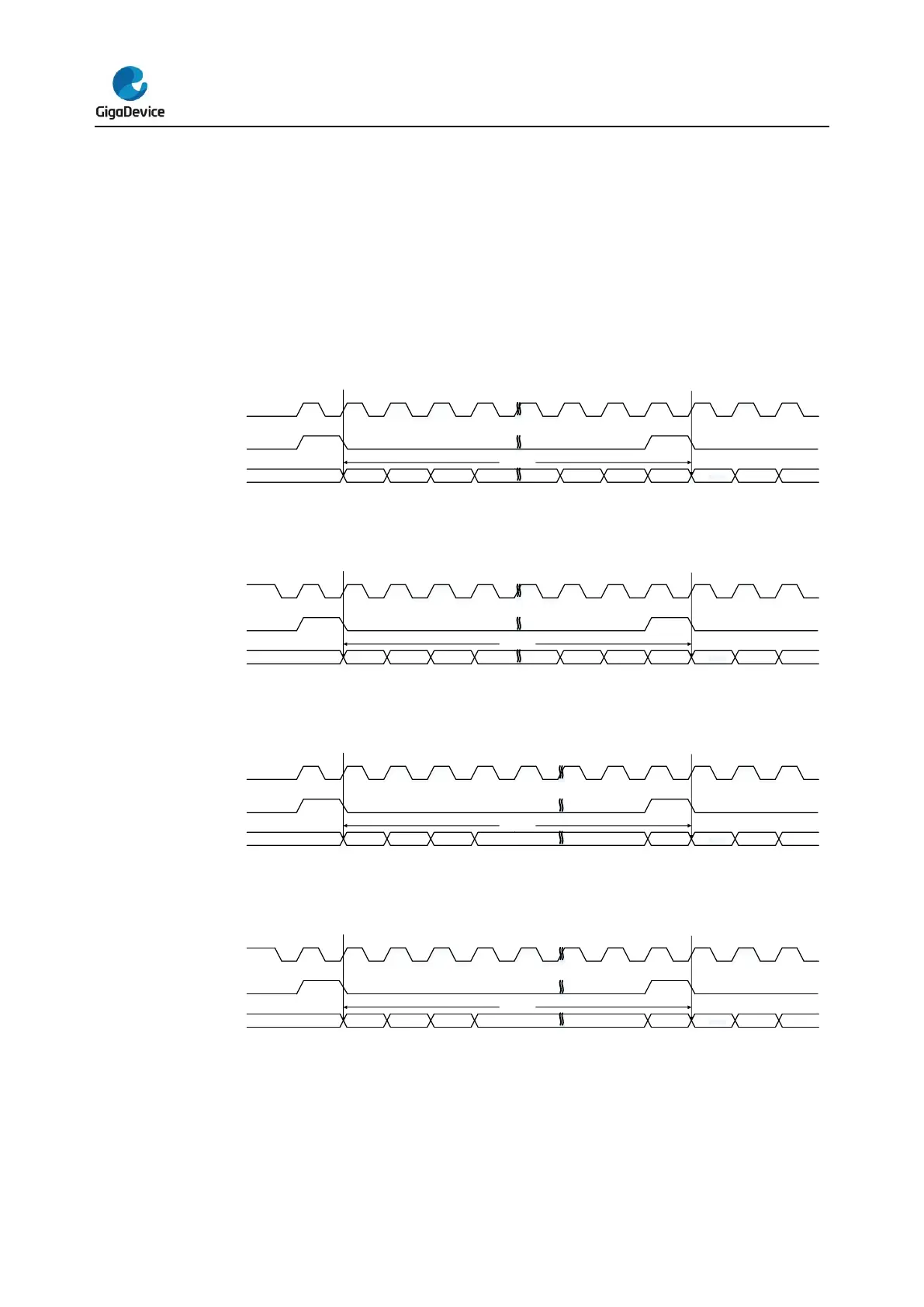
PCM standard
For PCM standard, I2S_WS and I2S_SD are updated on the rising edge of I2S_CK, and the
I2S_WS signal indicates frame synchronization information. Both the short frame
synchronization mode and the long frame synchronization mode are available and
configurable using the PCMSMOD bit in the SPI_I2SCTL register. The SPI_DATA register is
handled in the exactly same way as that for I2S Phillips standard. The timing diagrams for
each configuration of the short frame synchronization mode are shown below.
Figure 20-35. PCM standard short frame synchronization mode timing diagram
(DTLEN=00, CHLEN=0, CKPL=0)
Figure 20-36. PCM standard short frame synchronization mode timing diagram
(DTLEN=00, CHLEN=0, CKPL=1)
Figure 20-37. PCM standard short frame synchronization mode timing diagram
(DTLEN=10, CHLEN=1, CKPL=0)
Figure 20-38. PCM standard short frame synchronization mode timing diagram
(DTLEN=10, CHLEN=1, CKPL=1)
 Loading...

