GD32F3x0 User Manual
574
7. Buffer Time3
Buffer time with ASW_0 and ASW_1 open, PIN0 is configured to input floating.
8. Compare
ASW_0, ASW_1 and PIN0 remain the configuration of Step7. At this step, the voltage of
sample pin PIN1 is compared to a threshold called V
th
. If voltage of PIN1 is lower than V
th
,
the sequence returns to Step2 and continues, otherwise, the sequence ends.
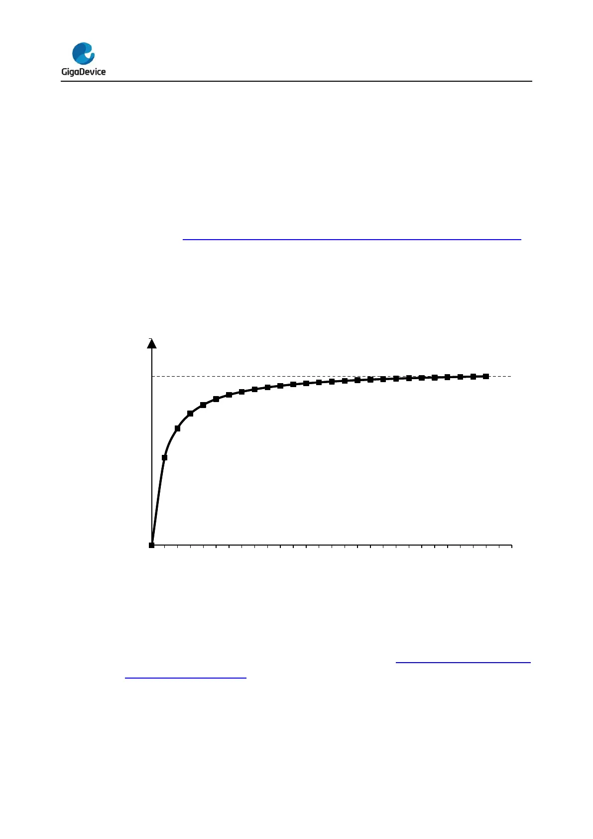
The voltage of sample pin V
s
is zero after initial step and increases after each charge cycle,
as shown in Figure 22-3. Voltage of a sample pin during charge-transfer sequence. A
larger C
x
will cause a greater increase during a cycle. The sequence stops when V
s
reaches V
th
. Each group has a counter which records the number of cycles performed on it
to reach V
th
. At the end of charge-transfer sequence, the group counter is read out to
estimate the C
x
, i.e. a smaller counter values indicates a larger C
x
.
Figure 22-3. Voltage of a sample pin during charge-transfer sequence
22.3.4. Charge transfer sequence FSM
A hardware Finite-state machine (FSM) is designed in chip to perform the charge transfer
sequence described in the previous section as shown in Figure 22-4. FSM flow of a
charge-transfer sequence.
 Loading...

