GD32F3x0 User Manual
31
1.6. System configuration registers (SYSCFG)
SYSCFG base address: 0x4001 0000
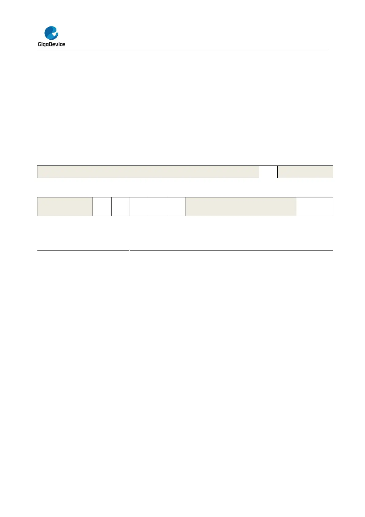
1.6.1. System configuration register 0 (SYSCFG_CFG0)
Address offset: 0x00
Reset value: 0x0000 000X (X indicates BOOT_MODE[1:0] may be any value according to
the BOOT0 pin and the BOOT1_n option bit after reset).
This register has to be accessed by word (32-bit).
Must be kept at reset value.
PB9 pin high current capability enable
When it is set, the PB9 pin can be used to control an infrared LED directly.
0: High current capability on the PB9 pin is enable.
1: High current capability on the PB9 pin is disabled, and the speed control of the
pin is bypassed.
Must be kept at reset value.
TIMER 16 DMA request remapping enable
0: Not remap (TIMER16_CH0 and TIMER16_UP DMA requests are mapped on
DMA channel 0)
1: Remap (TIMER16_CH0 and TIMER16_UP DMA requests are mapped on DMA
channel 1)
TIMER 15 DMA request remapping enable
0: Not remap (TIMER15_CH0 and TIMER15_UP DMA requests are mapped on
DMA channel 2)
1: Remap (TIMER15_CH0 and TIMER15_UP DMA requests are mapped on DMA
channel 3)
USART0_RX DMA request remapping enable
0: Not remap (USART0_RX DMA requests are mapped on DMA channel 2)
1: Remap (USART0_RX DMA requests are mapped on DMA channel 4)
 Loading...

