GD32F3x0 User Manual
598
Device mode
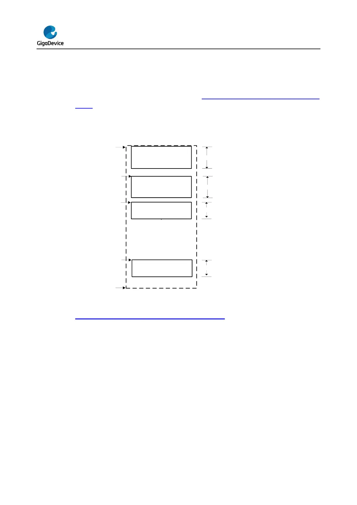
In device mode, the data FIFO is divided into several parts: one Rx FIFO and 4 Tx FIFOs
(one for each IN endpoint). All the OUT endpoints share the Rx FIFO for receiving packets.
The size and start offset of these data FIFOs should be configured using USBFS_GRFLEN
and USBFS_DIEPxTFLEN (x=0…3) registers. Figure 23-7. Device mode FIFO space in
SRAM describes the structure of these FIFOs in SRAM. The values in the figure are in term
of 32-bit words.
Figure 23-7. Device mode FIFO space in SRAM
USBFS provides a special register area for the internal data FIFO reading and writing.
Figure 23-8. Device mode FIFO access register map describes the register memory area
where the data FIFO can write. This area can be read by any endpoint FIFO. The addresses
in the figure are addressed in bytes. Each endpoint has its own FIFO access register space.
Rx FIFO is also able to be accessed using USBFS_GRSTATR/USBFS_GRSTATP register.


 To Next Page