GD32F3x0 User Manual
44
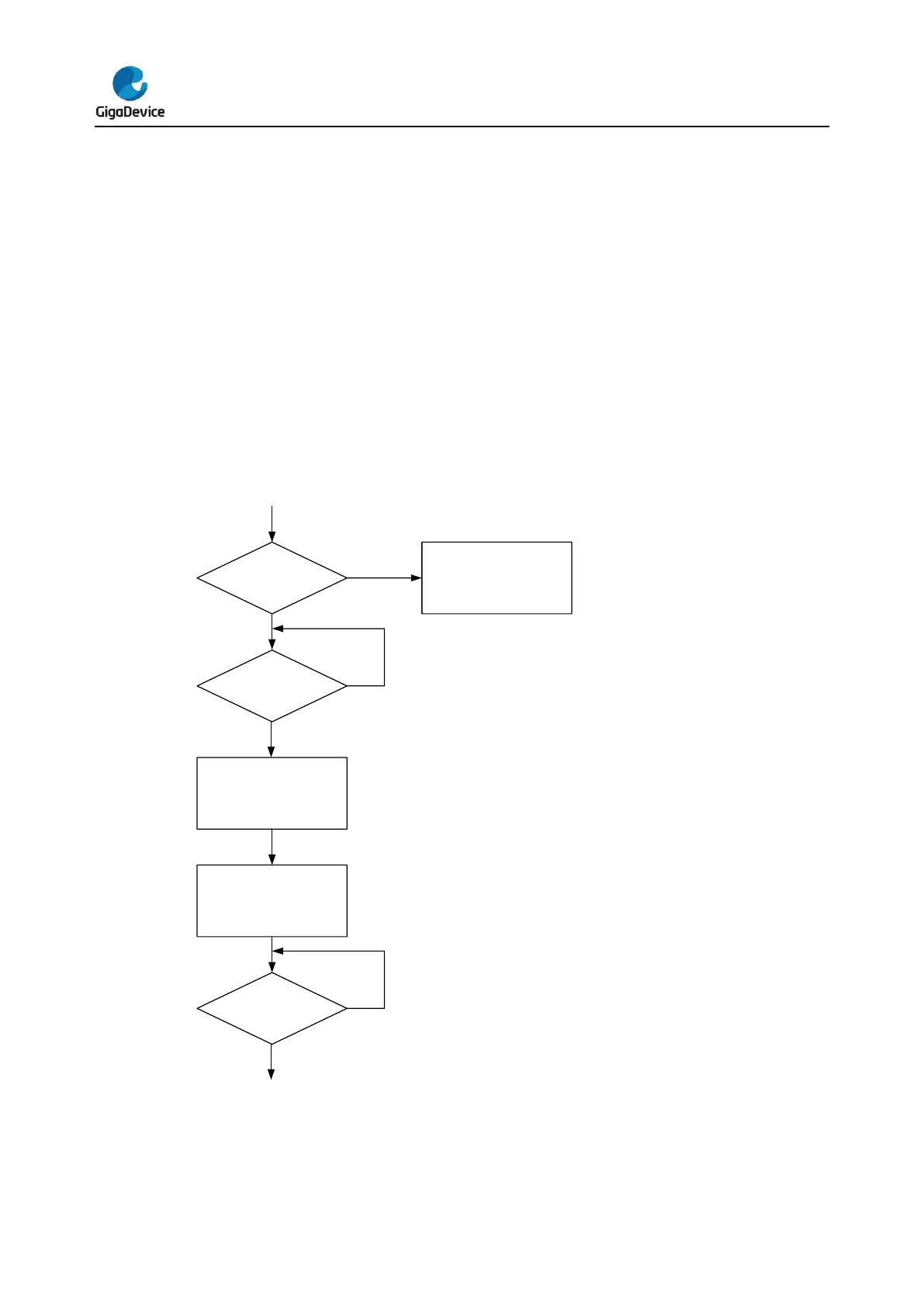
4. Send the mass erase command to the FMC by setting the START bit in FMC_CTL
register.
5. Wait until all the operations have been completed by checking the value of the BUSY bit
in FMC_STAT register.
6. Read and verify the flash memory by using a DBUS access if necessary.
When the operation is executed successfully, an interrupt will be triggered by FMC if the
ENDIE bit in the FMC_CTL register is set, and the ENDF in FMC_STAT register is set. Since
all flash data will be reset to a value of 0xFFFF FFFF, the mass erase operation can be
implemented by using a program that runs in SRAM or by using the debugging tool to access
the FMC registers directly. The end of this operation is indicated by the ENDF bit in the
FMC_STAT register. (The starting address of programming operation should be 0x0800
0000) The following figure indicates the mass erase operation flow.
Figure 2-2. Process of the mass erase operation