GD32F3x0 User Manual
550
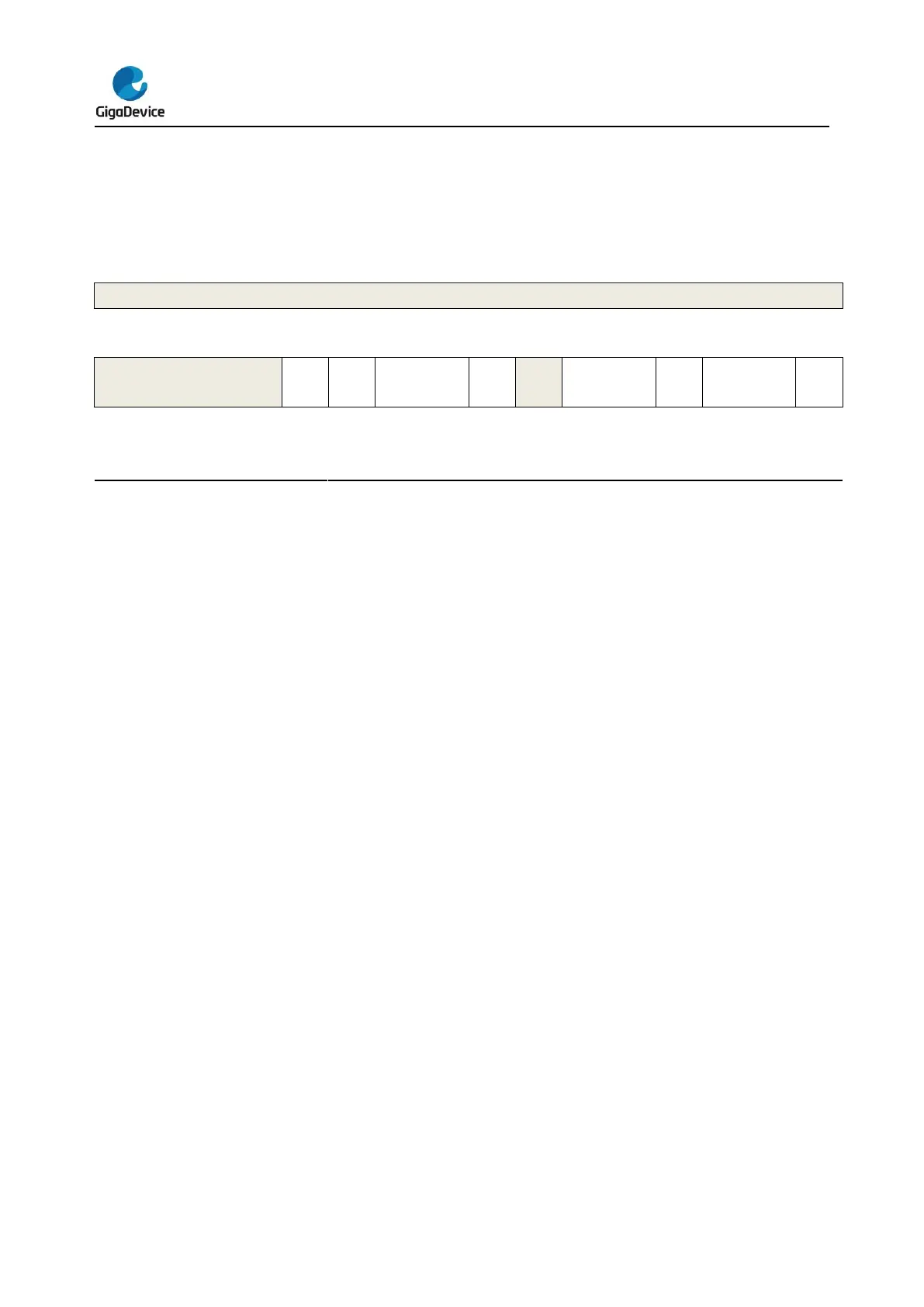
20.5.8. I I2S control register (SPI_I2SCTL)
Address offset: 0x1C
Reset value: 0x0000 0000
This register can be accessed by byte (8-bit) or half-word (16-bit) or word (32-bit).
Must be kept at reset value.
I2S mode selection
0: SPI mode
1: I2S mode
This bit should be configured when SPI mode or I2S mode is disabled.
I2S enable
0: Disable I2S
1: Enable I2S
This bit is not used in SPI mode.
I2S operation mode
00: Slave transmission mode
01: Slave reception mode
10: Master transmission mode
11: Master reception mode
This bit should be configured when I2S mode is disabled.
This bit is not used in SPI mode.
PCM frame synchronization mode
0: Short frame synchronization
1: long frame synchronization
This bit has a meaning only when PCM standard is used.
This bit should be configured when I2S mode is disabled.
This bit is not used in SPI mode.
Must be kept at reset value.
I2S standard selection
00: I2S Phillips standard
01: MSB justified standard
 Loading...

