Intel
®
EP80579 Integrated Processor Product Line—PCI Express* Interface
Intel
®
EP80579 Integrated Processor Product Line
Platform Design Guide May 2010
145 Order Number: 320068-005US
10.1.9 Topology 3 – EP80579 to PCI Express Down Device
Table 53 and Figure 94 summarize the layout routing solution space to a PCI Express
device on the board. In this case, EP80579 is a transmitter and the PCI Express device
is a receiver. All traces must be routed on the same layer.
• L1 starts from the EP80579 breakout region to the AC blocking capacitor via.
• L2 is the main routing section that is from the AC blocking capacitor via to the PCI
Express device breakout region.
• L3 is the breakout region of the PCI Express device.
• LT is the main routing section that is from the EP80579 pin to the PCI Express
device.
Trace Length L2, L2’ – to edge of logic
analyzer breakout region.
Min = 0.5 in.(stripline)
Min = 0.5 in. (microstrip)
Max = 5.5 in.(stripline)
Max = 6.0 in. (microstrip)
Figure 93
Trace Length L3, L3’ – Logic analyzer
breakout region.
Min = 3.5 in. (microstrip)
Max = 0.5 in. (stripline)
Max = 7.0 in. (microstrip)
Figure 93
Trace Length L4, L4’ – Logic analyzer
breakout region.
Max = 0.5 in. (stripline) Figure 93
Trace Length L5, L5’ – Logic analyzer
breakout region to PCI Express connector.
Min = 2.5 in. (stripline)
Max = 7.0 in. (stripline)
Figure 93
Trace Length LT– EP80579 pin to PCI
Express connector
LT = L1 + L2 +L3 + L4 + L5 (stripline)
LT = L1 + L2 +L3 (microstrip)
Figure 93
AC Blocking Capacitor–AC CAP 0.1 μF Figure 93
Length Tuning Requirements
Routing must remain on the same layer.
Maximum number of vias is 6 (stripline) and 4
(microstrip).
LT-LT’ = ±5 mils
Figure 93
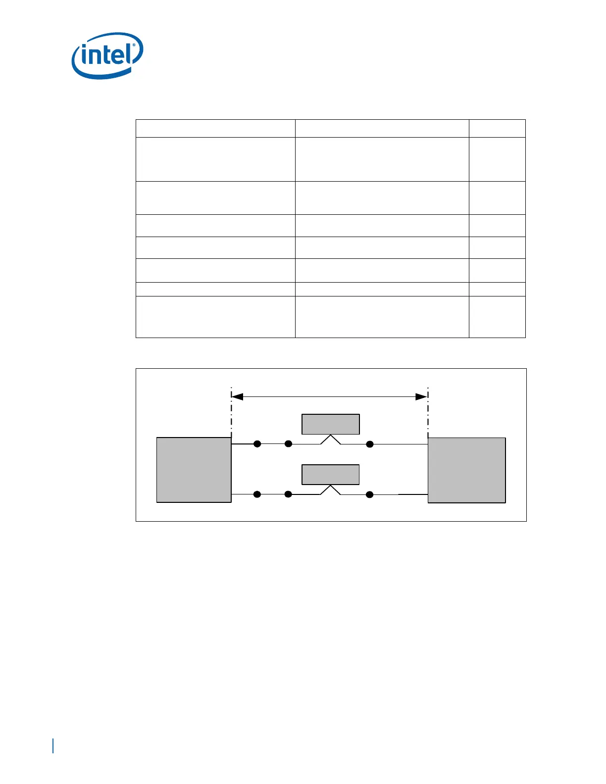
Figure 93. PCI Express Connector With LAI Connector Routing (EP80579 Receive)
Table 52. PCI Express Connector with LAI Connector Routing (EP80579 Receive) (Sheet
2 of 2)
Parameter Routing Guidelines Figure
EP80579
PCI
Express*
Connector
L1
LT = L1 + L2 + L3 + L4 + L5
LAI
Connector
L4L3 L5
L1'
LAI
Connector
L4'L3' L5'
L2
L2'