Intel
®
EP80579 Integrated Processor Product Line—System Memory Interface (DIMM)
Intel
®
EP80579 Integrated Processor Product Line
Platform Design Guide May 2010
123 Order Number: 320068-005US
9.7.1.2 DDR2 Clock Group Signals - DDR_CLK[5:0]/DDR_CLK#[5:0]
The clock signal group includes six differential clock pairs per channel. The EP80579
generates and drives these differential clock signals. Since the EP80579 supports both
registered and unbuffered DDR2 DIMMs, three separate differential clock pairs are
routed to each DIMM connector. Table 40 summarizes the clock signal mapping, and
Figure 79 shows the clock interconnect between the EP80579 and the DIMMs.
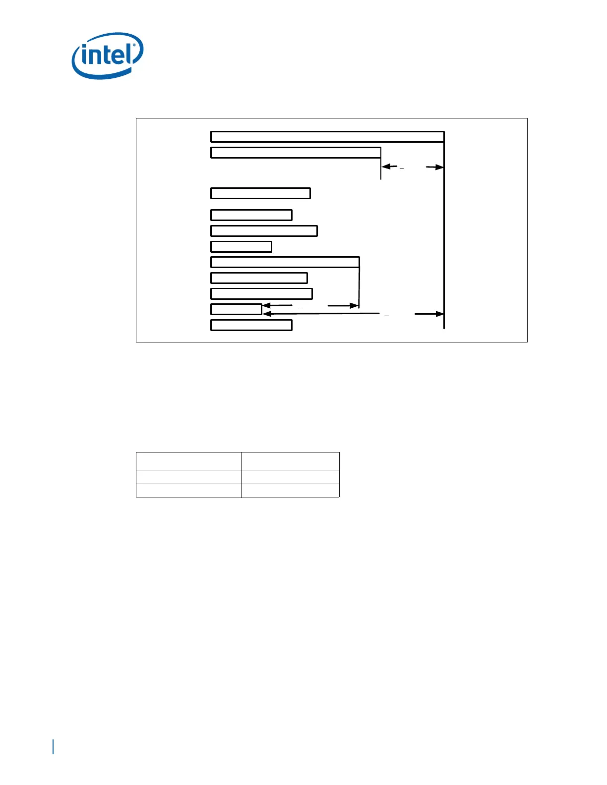
Figure 78. Example Length Matching for a Data Byte Lane
DDR_DQS#[0]
DDR_DQS[0]
DDR_DQ[1]
DDR_DQ[0]
DDR_DQ[7]
DDR_DQ[5]
DDR_DQ[6]
DDR_DQ[4]
DDR_DQ[3]
DDR_DQ[2]
DDR_DM[0]
<
400 mil
<
20 mil
<
10 mil
Table 40. Differential Clock Signal Mapping
Signal Relative To
CLK[2:0], CLK#[2:0] DIMM0
CLK[5:3], CLK#[5:3] DIMM1

 Loading...


