Intel
®
EP80579 Integrated Processor Product Line—Platform System Clock
Intel
®
EP80579 Integrated Processor Product Line
Platform Design Guide May 2010
97 Order Number: 320068-005US
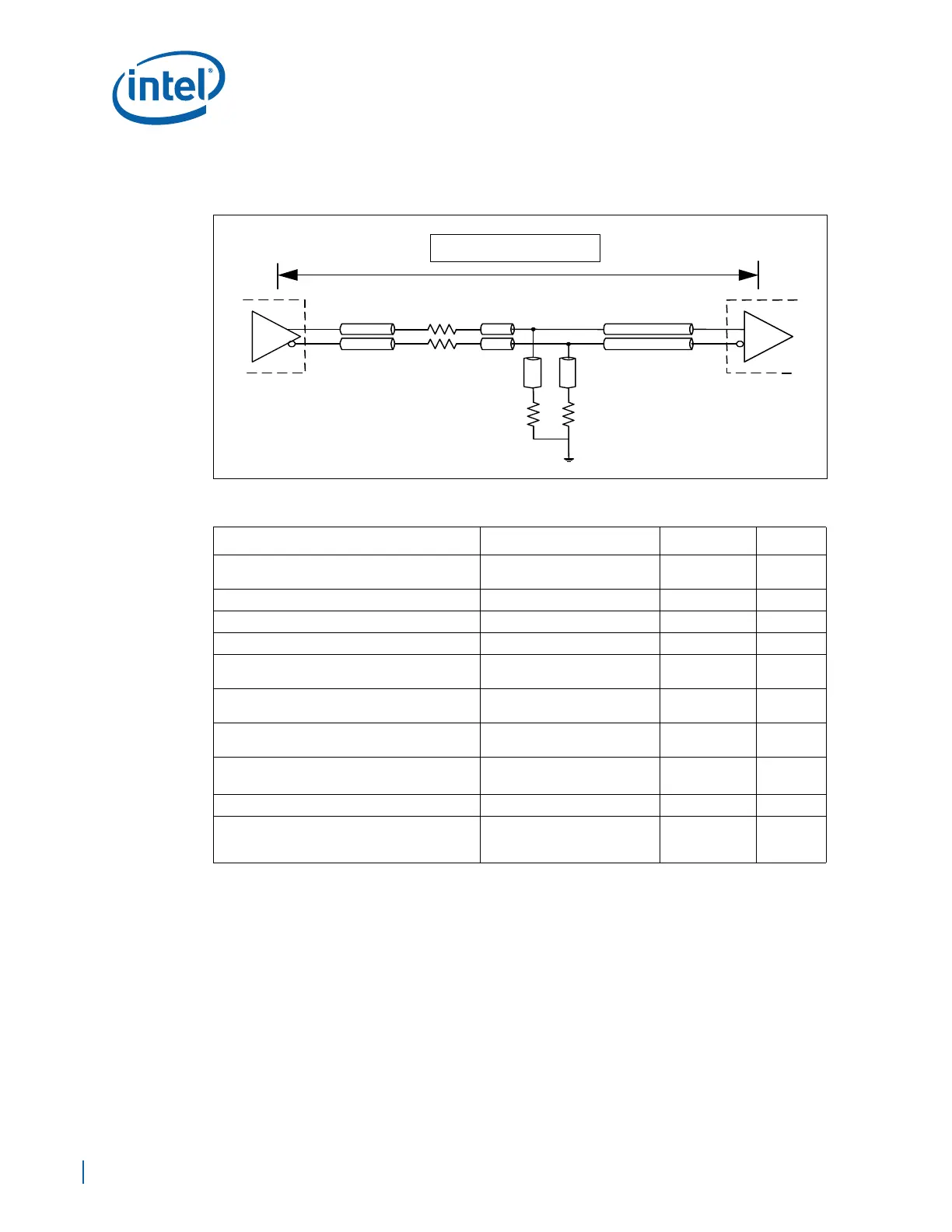
8.2.2.3 Source Clock to Down Devices
Figure 55. Source Clock Topology to Down Devices (Except PCI-E)
Table 19. 100 MHz SRC/SRC# Clock Routing Guidelines for Down Devices(Except PCI-E)
Layout Guideline Value Figure Notes
Trace Width (W) microstrip: 4.5 mils
stripline: 4.75 mils
Figure 57 1,2
Differential Pair Spacing (S) 10 mils Figure 57 3,4
Spacing to Other Traces (S1) 20 mils Figure 57
Motherboard Impedance – Differential 100
Ω ±10% 3,4
Routing Length (L1, L1’):
Clock Driver to Rs
0.5in. max
Figure 55 5
Routing Length (L2, L2’):
Rs to Rs-Rt Node
0.2in. max
Figure 55 5
Routing Length (L3, L3’):
Rs-Rt Node to Rt
0.2in. max
Figure 55 5
Routing Length (L4, L4’):
Rs-Rt Node to Load
Min: 1in.
Max: 16in.
Figure 55
SRC to SRC# Length Matching within 5 mils
Resistors Rs = 22-33
Ω ±5%
Rt = 49.9
Ω ±1% (for 100 Ω
differential impedance)
Figure 55
Notes:
1. Routing guidelines are for the width is 4.5 mils with 10 mil spacing on layers 3 & 8. Use 4.5-mil line
width and adjust the trace to trace air gap to achieve 100 Ω differential impedance.
2. Trace width and differential spacing is stackup dependent.
3. Clock traces are routed in a differential configuration. Maintain the minimum recommended spacing
between the two traces of the pair. Maintain uniform spacing along the entire length of the trace. Do
not exceed the maximum trace spacing, as this will degrade the noise rejection of the network.
4. The differential impedance of each clock pair is the critical parameter. Single-ended impedance may
vary with different geometries.
5. Minimize L1, L2 and L3 lengths. Long lengths on L2 and L3 degrade effectiveness of source
termination and contribute to ringback.
L1'
L1
Rs
L2
L2'
L3
L3'
L4
L4'
Clock Driver
CK410
SATA, or other
down devices
(Except PCI-E)
Rs
Rt Rt
LT = L1 + L2 + L4