Intel
®
EP80579 Integrated Processor Product Line—System Memory Interface (DIMM)
Intel
®
EP80579 Integrated Processor Product Line
Platform Design Guide May 2010
131 Order Number: 320068-005US
9.7.2 Reset Pin Requirement
Board designers must connect the DIMM pin 18 (RESET#) to the PWRGOOD signal from
the voltage regulator that provides 1.8 V power to that DIMM. This signal must conform
to standard SSTL_18 signaling levels. The DIMM RESET# input must not go low for any
reason once the power up sequence is complete. The EP80579 drives all clock enables
low by default as it comes out of power up. The timing of the PWRGOOD signal must be
such that EP80579 is safely driving DDR_CKE low when PWRGOOD transitions from low
to high.
9.7.3 DC Bias Signals
The DC bias signals consist of DDR_SLWCRES, DDR_RCOMPX, DDR_CRES[2:0],
DDV_CRES, and DDR_VREF. The routing guidelines for these signals are described in
the following sections.
9.7.3.1 DDR_SLWCRES, DDR_RCOMPX, DRV_CRES, & DDR_CRES0
The DDR_SLWCRES, DDR_RCOMPX, DRV_CRES, and DDR_CRES0 signals are
compensation resistors for slew rate, impedance, and common return, respectively.
Intel recommends 20 mil wide traces with a minimum spacing of 12 mils from other
signals. When breaking out from the EP80579, maintain a minimum spacing of 4.5 mils
up to a maximum length of 500 mils. For the best signal integrity, minimize this length
as much as possible. Figure 83 shows the routing topology for these signals.
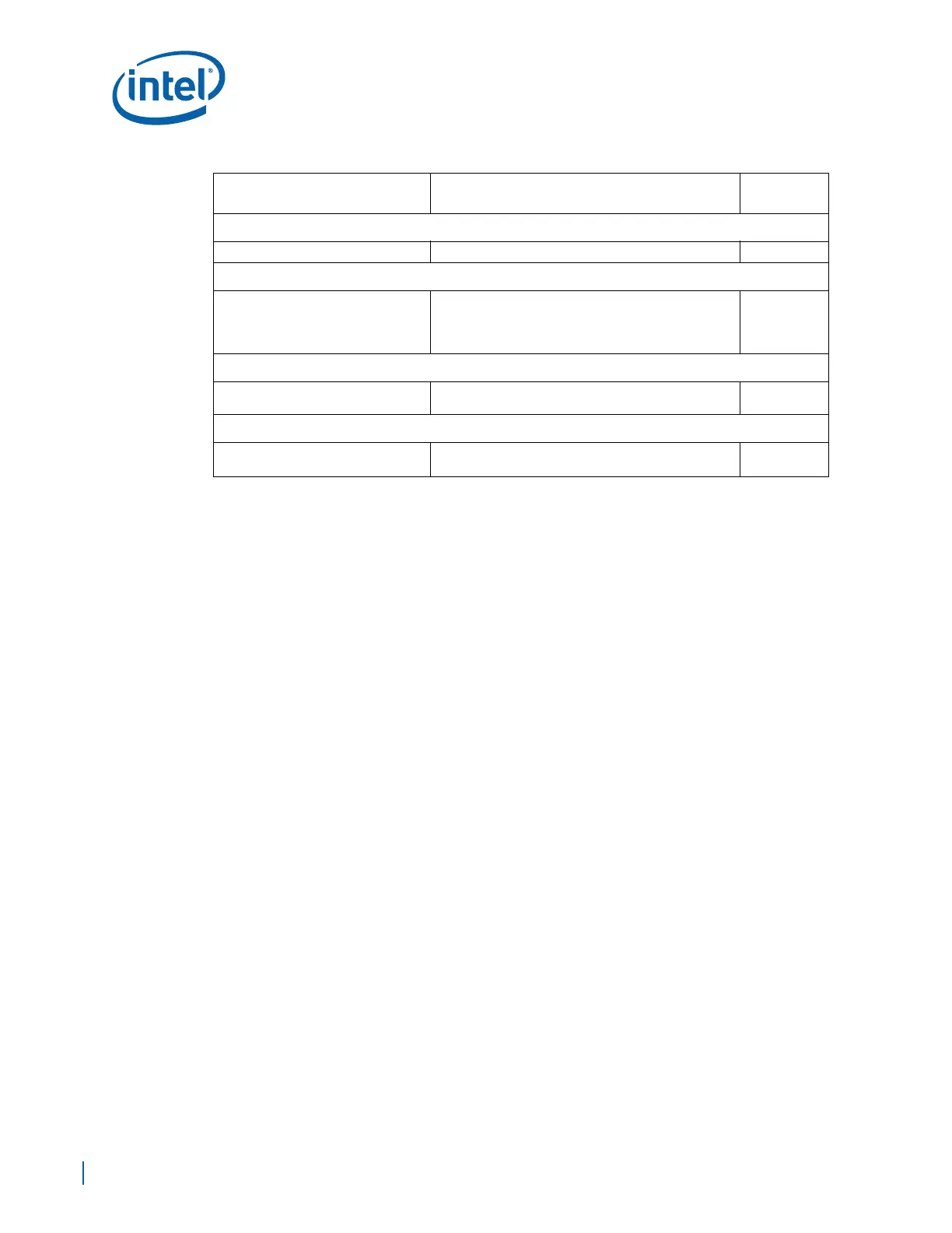
On-Board Termination
Parallel Termination Resistor (Rtt) 60 Ω ±1% Figure 82
DIMM Compensation Capacitor
DIMM0 Compensation Capacitor
(Ccomp)
18pF
• One capacitor per ADD/CMD signal to DIMM0
only. Place capacitor as close as possible to
DIMM0.
Figure 82
Length/Skew Matching Rules
Length Tuning Requirements
• ADD/CMD signals should match in length within
20 mils of each other.
Routing Rules
CLK-to-ADD/CMD Requirements
Clock signals should match ADD/CMD signals, in
length, within 20 mils max.
Table 46. DDR2 Address/Command Signal Group Routing Guidelines (Sheet 2 of 2)
Parameter
Routing Guidelines for 2-DIMM Solution with
ODT
Figure