Intel
®
EP80579 Integrated Processor Product Line—PCI Express* Interface
Intel
®
EP80579 Integrated Processor Product Line
Platform Design Guide May 2010
147 Order Number: 320068-005US
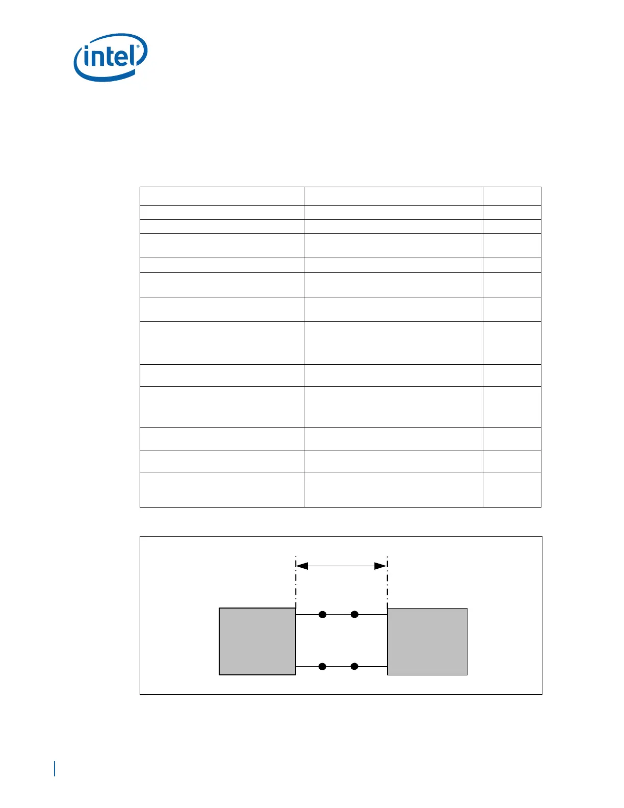
• L2 starts from the EP80579 breakout region to the PCI Express device breakout
region.
• L3 is the breakout region of the PCI Express device.
• LT is the main routing section that is from the EP80579 pin to the PCI Express
device.
Table 54. PCI Express Down Device Routing (EP80579 Receive)
Parameter Routing Guidelines Figure
Signal Group PEA0_Tn[7:0], PEA0_Tp[7:0] -
Reference Plane Ground Referenced -
Layer Assignment
Layers 3 or 8 (stripline)
Layers 1 or 10 (microstrip)
-
Characteristic Trace Impedance (Zo) 90 Ω ±10% (Differential) -
Nominal Trace Width
4.5 mils (stripline)
4.75 mils (microstrip)
Figure 87
Figure 88
Nominal Trace Spacing within a pair from
edge to edge
5.5 mils (stripline)
5.25 mils (microstrip)
Figure 87
Figure 88
Nominal Trace Spacing from edge of one
differential pair to edge of another
differential pair
The greater of:
• 18 mils or 3x dielectric thickness (stripline)
• 20 mils or 3x dielectric thickness
(microstrip)
Figure 87
Figure 88
Trace Length L1, L1’– EP80579 Breakout
region
Min = 0.75 in.
Max = 2.5 in.
Figure 95
Trace Length L2, L2’ – edge of EP80579
Breakout region to edge PCI Express
Device breakout region.
Min = 4.0 in (stripline)
Min = 2.5 in (microstrip)
Max = 14.5 in. (stripline)
Max = 13.0 in. (microstrip)
Figure 95
Trace Length L3, L3’ – PCI Express
breakout region.
Min = 0.75 in.
Max = 2.0 in.
Figure 95
Trace Length LT– EP80579 pin to PCI
Express connector
LT = L1 + L2 +L3 Figure 95
Length Tuning Requirements
Routing must remain on the same layer.
Maximum number of vias is 4.
LT-LT’ = ±5 mils
Figure 95
Figure 95. PCI Express Down Device Routing (EP80579 Receive)
EP80579
PCI
Express*
Device
L1
LT = L1+L2+L3
L3
L1'
L3'
L2
L2'