Intel
®
EP80579 Integrated Processor Product Line—System Memory Interface (SODIMM)
Intel
®
EP80579 Integrated Processor Product Line
Platform Design Guide May 2010
324 Order Number: 320068-005US
A.4.5.2 DDR2 Clock Group Signals - DDR_CLK[1:0]/DDR_CLK#[1:0]
The clock signal group for the SODIMM comprises of two differential clock pairs. The
differential clock pairs must be point-to-point routed from the EP80579 to the SODIMM
and must maintain the correct isolation spacing from other signals. Additionally, it is
important to maintain the correct spacing and length matching between the pair to
protect the differential integrity.
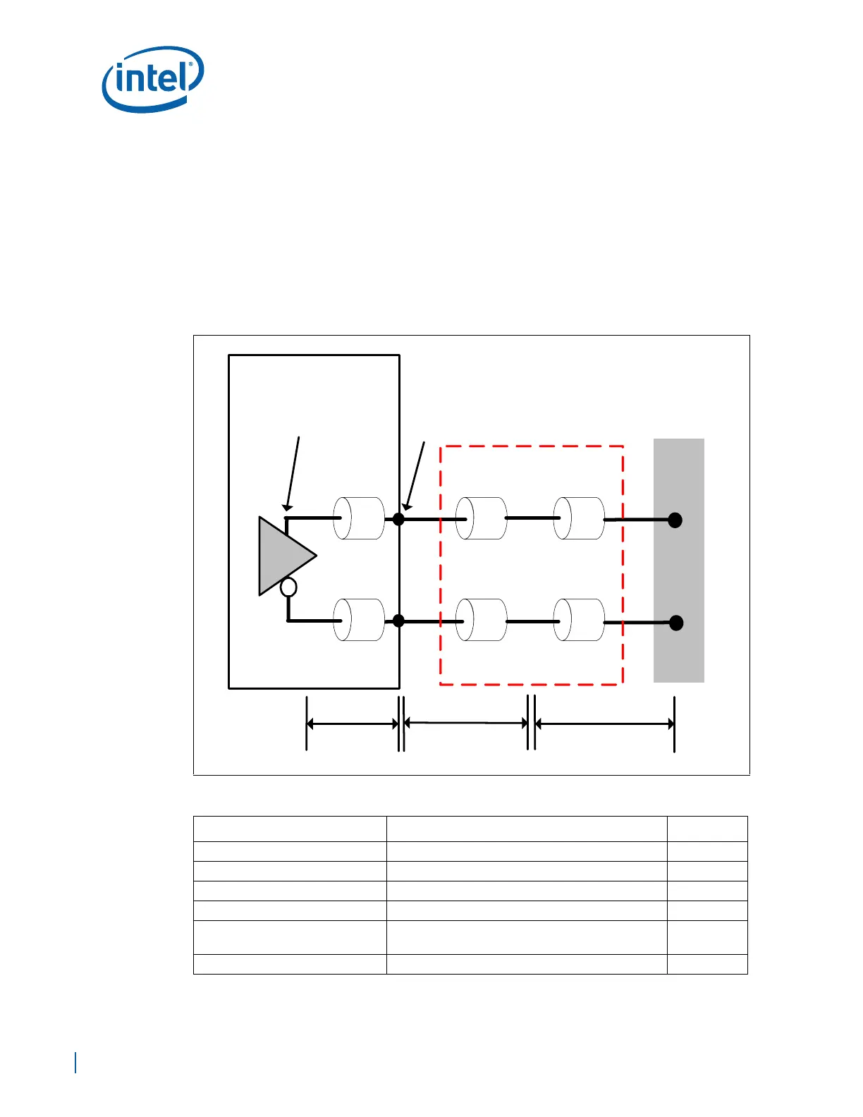
Figure A-3 and Table A-7 depict the recommended topology and layout routing
guidelines for the DDR2 differential clocks. Route differential pair signals on the same
layer. No external terminations are required for the clock signals because they are
terminated on the SODIMM.
Figure A-3. DDR2 Point-to-Point Clock Routing Diagram
Table A-7. Clock Signal Group Routing Guidelines (Sheet 1 of 2)
Parameter Routing Guidelines for SODIMM Figure
Signal Group CLK/CLK#[1:0] - SODIMM
Topology Point-to-Point (Differential) Figure A-3
Reference Plane Ground Referenced
Layer Assignment Layers 3/8 (Route Clock group on the same layer)
Characteristic Trace Impedance (Zo)
Single Ended Impedance:
40Ω ±10%
Figure A-3
Nominal Trace Width 6.5 mils for L3/L8 Figure A-3
SODIMM
EP80579
L
PKG
L
BREAKOUT
L
ROUTE
EP80579 Pin
Breakout
Routing
EP80579
Pad
Board
Routing
B
C
A#
B#
C#
Package
Trace
A
Differential