Intel
®
EP80579 Integrated Processor Product Line—System Memory Interface (SODIMM)
Intel
®
EP80579 Integrated Processor Product Line
Platform Design Guide May 2010
318 Order Number: 320068-005US
A.4 SODIMM System Memory Design Guidelines
This section provides an example of the solution space as a result from simulation.
These simulation results have not been physically validated by Intel and is to be
used for reference purposes only. The values suggested in this section (resistor,
trace length, breakout length, etc.) may not provide the only possible solution space.
There can be different setups that may be equally feasible. Thorough simulations,
careful layout implementation, and vigorous stress testing and validation must be
performed to ensure that the design is robust if other design options are considered.
A.4.1 SODIMM DDR2 Signal Groups
The EP80579 has a single channel memory interface. The channel consists of 64 data
bits with no ECC support. The pinout for the channel has been optimized for a
baseboard design with one SODIMM.
The system memory interface can be divided into five signal groups:
• source synchronous (data)
• address/command
•control
•clocks
• DC bias signals
Table A-4 summarizes the different signal groupings:
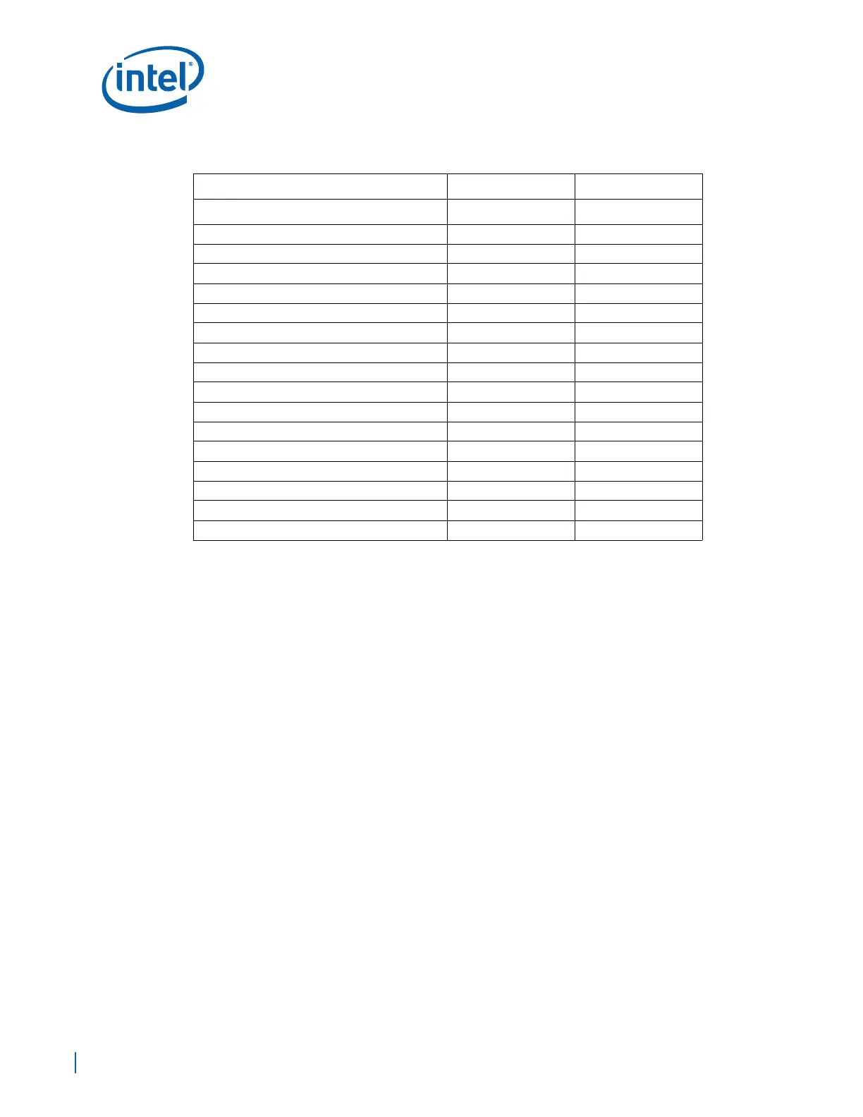
Table A-3. DDR2 Unbuffered SODIMM and Unbuffered DIMM Pin Comparison Table
SODIMM (200 pins) DIMM (240 pins)
Signal # of pins # of pins
VDD (SDRAM Core Power Supply) 12 12
VDDQ (SDRAM I/O Driver Power Supply) 010
VREF (SDRAM I/O Reference Power Supply) 11
VSS (Ground) 57 64
DQ (SDRAM Memory Data Bus) 64 64
DQS/DQS# (SDRAM Data Strobes) 16 18
DM (SDRAM Data Masks) 89
ECC (SDRAM ECC Check Bits) 08
CK/CK# (SDRAM Clocks) 46
Address (SDRAM Address Bus) 19 19
CMD (SDRAM Command Signals) 33
CS#/CKE (Chip Select and Clock Enable) 44
ODT (On die Termination) 22
SPD (Serial Presence Detect) 56
NC/RC/TEST 521
Total 200 240

 Loading...


