Intel
®
EP80579 Integrated Processor Product Line May 2010
Order Number: 320068-005US 120
System Memory Interface (DIMM)—Intel
®
EP80579 Integrated Processor Product Line
9.7.1 Topologies and Routing Guidelines
9.7.1.1 DDR2 Data and Strobe Signals – DQ/DM/ECC/DQS
The Data and Strobe topology shown in Figure 76 and Figure 77 is the same for each
Data Byte Group (See Table 37). The DQS signals must be routed as differential pair
with a skew between of ± 10mils. All signals in same byte lane should be matched
within 20 mils of each other. (For example, DQS0[+/-], DQ[0..7] and DM0 are in the
same byte lane).
All trace impedances should be 40 ohm± 10%. The parameters provided in Table 39
are targeted for 40 ohm.
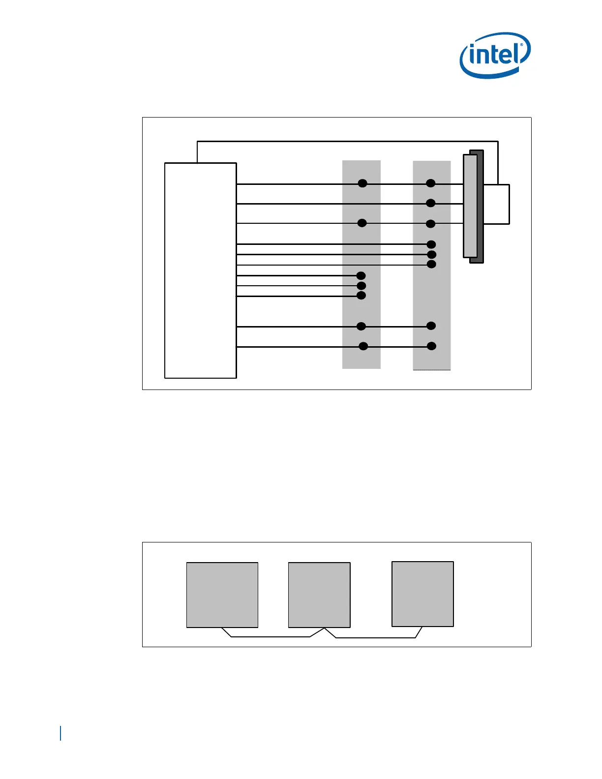
Figure 75. DDR2 Interfaced System Interconnect
DIMM 0
EP80579
DIMM 1
Parallel Termination Resistors
VTT
Regulator
Command/Address
CS0#, CKE0, ODT0
CS1#, CKE1, ODT1
DDR2_VTT
DDR2
Memory
Controller
CLK0, CLK0#
CLK1, CLK1#
CLK2, CLK2#
CLK3, CLK3#
CLK4, CLK4#
CLK5, CLK5#
DQS[8:0]/DQS#[8:0]
DQ[63:0], DM[8:0], ECC[7:0]
Figure 76. Data Signal Daisy Chain Routing Topology

 Loading...


