Intel
®
EP80579 Integrated Processor Product Line May 2010
Order Number: 320068-005US 344
System Memory Interface (Memory Down)—Intel
®
EP80579 Integrated Processor Product Line
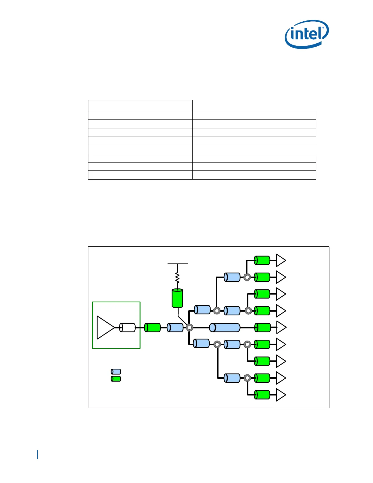
B.6.5 Address, Command and Control Signals
The address, command and control signals shown in Table B-30 are source-clocked
signals.
The address, command and control signals are source-clocked signals. The signals are
“clocked” into the SDRAM devices using the positive edge of the clock signals. The
EP80579 drives the address/command and clock signals together.
Figure B-26, and Table B-31 show the recommended topology and layout routing
guidelines for the DDR2-SDRAM address, command and control signals. A maximum of
6 vias should be used for layer changes over the entire route from the EP80579 pin to
SDRAM pin.
Table B-30. Address and Command Signals
Signal Description Signal Name
System Memory Address Signals DDR_MA[14:0]
Bank Addresses DDR_BA[2:0]
Row Address Select DDR_RAS#
Column Address Select DDR_CAS#
Write Enable DDR_WE#
Chip Select DDR_CS[0]#
Clock Enable DDR_CKE[0]
On-Die-Termination (ODT) DDR_ODT[0]
Figure B-12. DDR2 Address, Command and Control Signal Routing Topology
DDR_VTT
L4
L4
L4
L4
L4
L4
L4
L4
Pkg
EP80579
= Stripline Routing
= Microstrip Routing
TL1
Rtt
L4
L4
SDRAM-ECC
SDRAM4
SDRAM5
SDRAM6
SDRAM7
SDRAM0
SDRAM1
SDRAM2
SDRAM3
Lp
L3
L3
L3
L3
L2
L2
L1L0 L-ECC

 Loading...


