Intel
®
EP80579 Integrated Processor Product Line—System Memory Interface (DIMM)
Intel
®
EP80579 Integrated Processor Product Line
Platform Design Guide May 2010
125 Order Number: 320068-005US
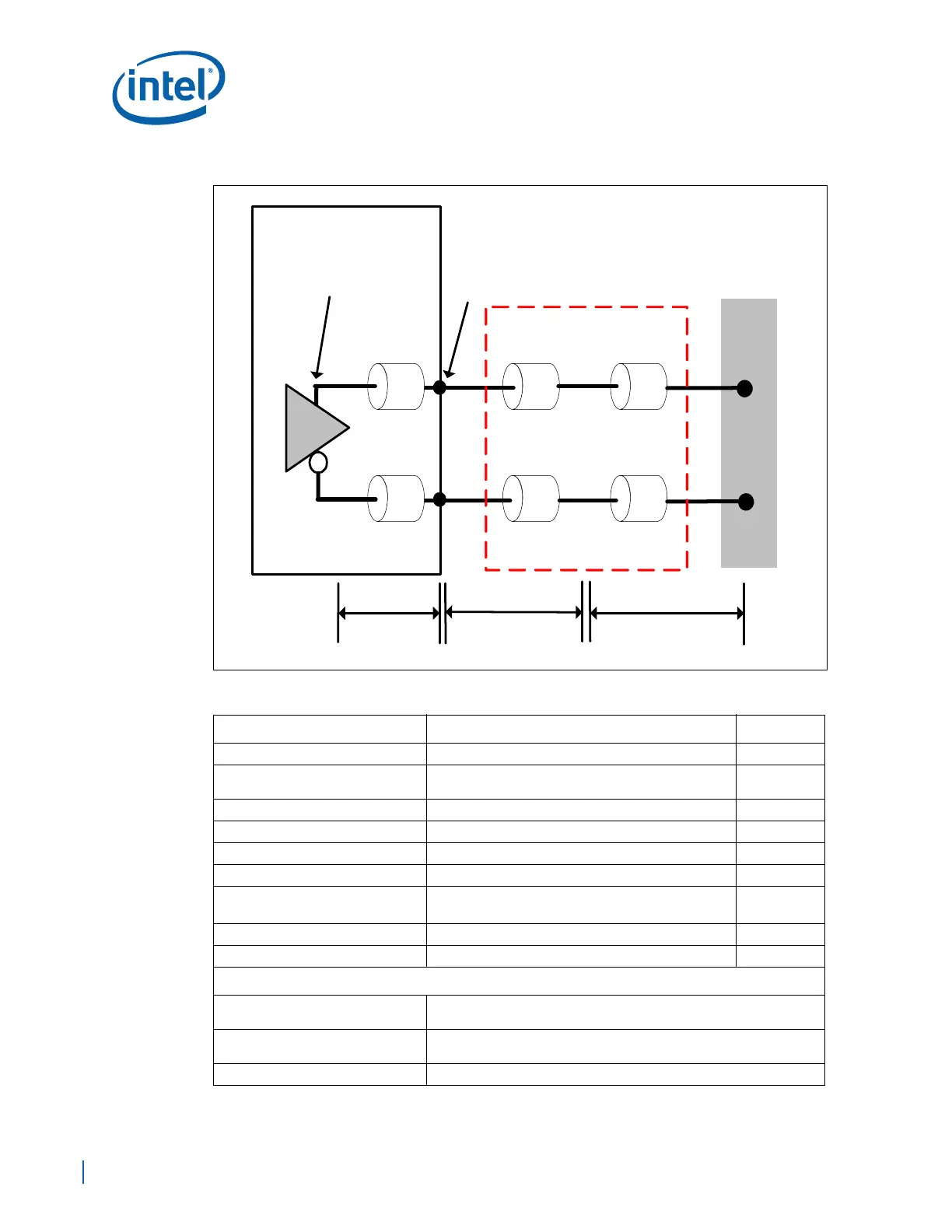
Figure 80. DDR2 Point-to-Point Clock Routing Diagram
Table 41. Clock Signal Group Routing Guidelines (Sheet 1 of 2)
Parameter Routing Guidelines for 2-DIMM Solution Figure
Signal Group CLK/CLK#[2:0] - DIMM0; CLK/CLK#[5:3] -DIMM1 Figure 79
Topology Point-to-Point
Figure 79,
Figure 80
Reference Plane Ground Referenced
Layer Assignment Layers 3/8 (Route Clock group on the same layer)
Characteristic Trace Impedance (Zo) Single Ended Impedance: 40Ω ±10% Figure 80
Nominal Trace Width 6.5 mils for L3/L8 Figure 80,
Inter-pair Trace Spacing(e2e)
(CLK to CLK# spacing)
6.0 mils Figure 80
Pair-to-Pair Spacing (e2e) 15.0 mils
Clearance from other signals groups 20.0 mils Figure 80
Board Routing Guidelines
Total Trace Length (TTL) = (L
PKG
+
L
BREAK
+ L
ROUTE
)
2.0 in - 6.0 in
L
PKG
See the Intel
®
EP80579 Integrated Processor Product Line Datasheet
for package length information
L
BREAK
Max = 0.8 in
DIMM
EP80579
L
PKG
L
BREAK
L
ROUTE
EP80579 Pin
Breakout
Routing
EP80579
Pad
Board
Routing
B
C
A#
B#
C#
Package
Trace
A
Differential

 Loading...


