Intel
®
EP80579 Integrated Processor Product Line May 2010
Order Number: 320068-005US 327
System Memory Interface (SODIMM)—Intel
®
EP80579 Integrated Processor Product Line
A.4.5.4 Address and Command Signals – DDR_MA[14:0],
DDR_BA[2:0], DDR_RAS#, DDR_CAS#, DDR_WE#
The address/command signals shown in Table A-11 are source-clocked signals.
The address/command signals are source-clocked signals that include 15 system
memory address signals (MA[14:0]), 3 bank addresses (BA[2:0]), row address select
(RAS#), column address select (CAS#), and write enable (WE#). The address/
command signals are “clocked” into the SODIMM using the positive edge of the
differential clock signals. The EP80579 drives the address/command and clock signals
together.
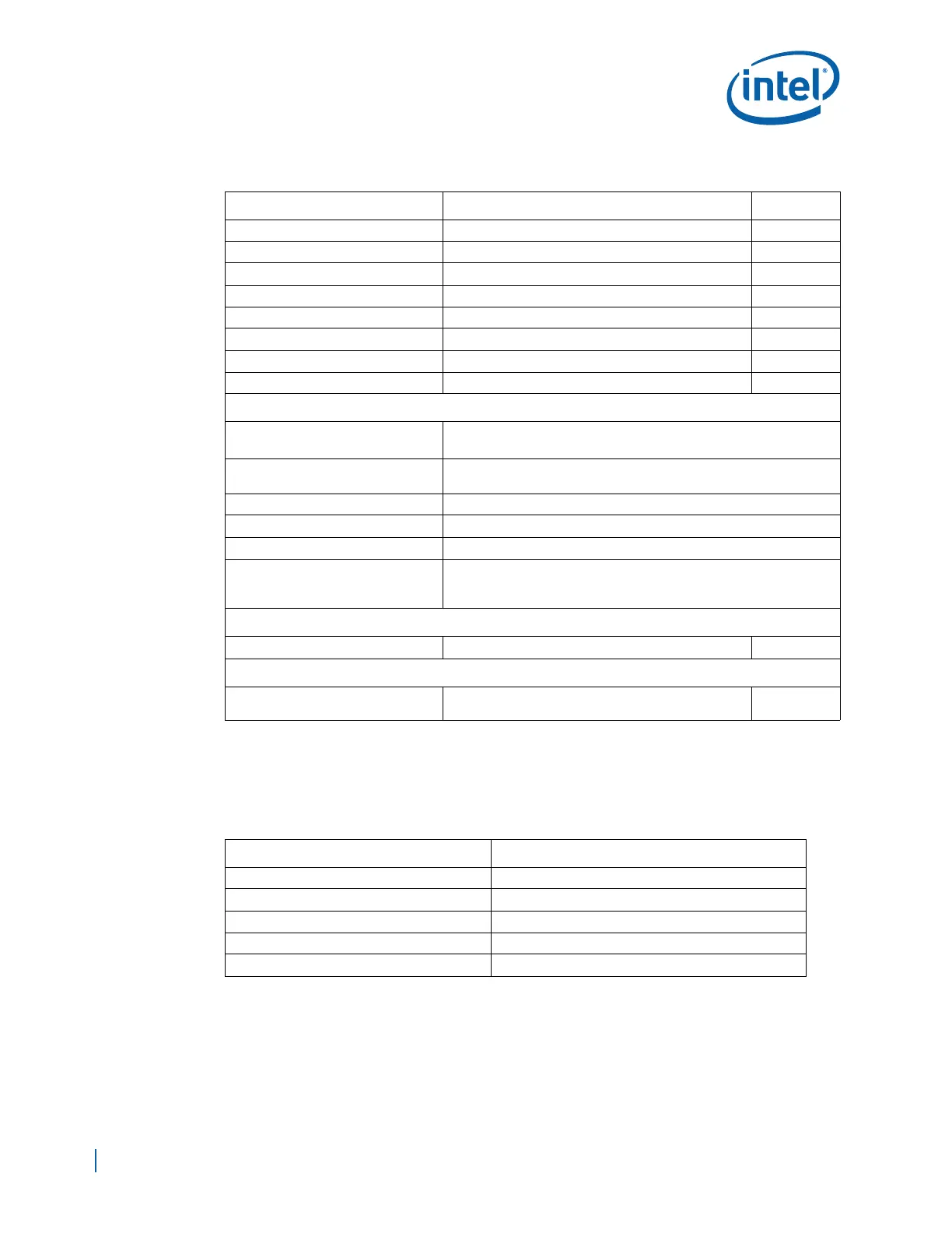
Table A-10. DDR2 Control Signal Group Routing Guidelines
Parameter Routing Guidelines for SODIMM Figure
Signal Group Control Signals (CS#/ODT/CKE)
Topology Point-to-Point
Reference Plane Ground Referenced
Layer Assignment Layers 3/8
Characteristic Trace Impedance (Zo) 40 Ω ±10% Figure A-4
Nominal Trace Width 6.5 mils Figure A-4
Nominal Trace Spacing (e2e) 3X Trace Width Figure A-4
Clearance from other signals 20 mils (min)
Board Routing Guidelines
Total Trace Length (TTL) = (L
PKG
+
L
BREAKOUT
+ L
ROUTE
+ L
BREAKIN
)
• TTL (CTRL) = 1.0 in - 7.5 in
• TTL (CTRL) = TTL (CMD/ADD) + 3 in
L
PKG
See the Intel
®
EP80579 Integrated Processor Product Line Datasheet
for package length information.
L
BREAKOUT
Max = 0.8 in
L
ROUTE
Max = 6.5 in
L
BREAKIN
Max = 0.8 in
L
TERM
Max = 500 mils
• Trace length skews for the control signals to the termination
resistors (L
TERM
) should not exceed 200 mils.
On-Board Termination
Parallel Termination Resistor (Rtt) 75 Ω ±1% Figure A-4
Length/Skew Matching Rules
Length Tuning Requirements
• The control signals need to match in length within
± 20 mils of each other.
Table A-11. Address and Command Signals
Signal Description Signal Name
System Memory Address Signals DDR_MA[14:0]
Bank Addresses DDR_BA[2:0]
Row Address Select DDR_RAS#
Column Address Select DDR_CAS#
Write Enable DDR_WE#