Intel
®
EP80579 Integrated Processor Product Line May 2010
Order Number: 320068-005US 144
PCI Express* Interface—Intel
®
EP80579 Integrated Processor Product Line
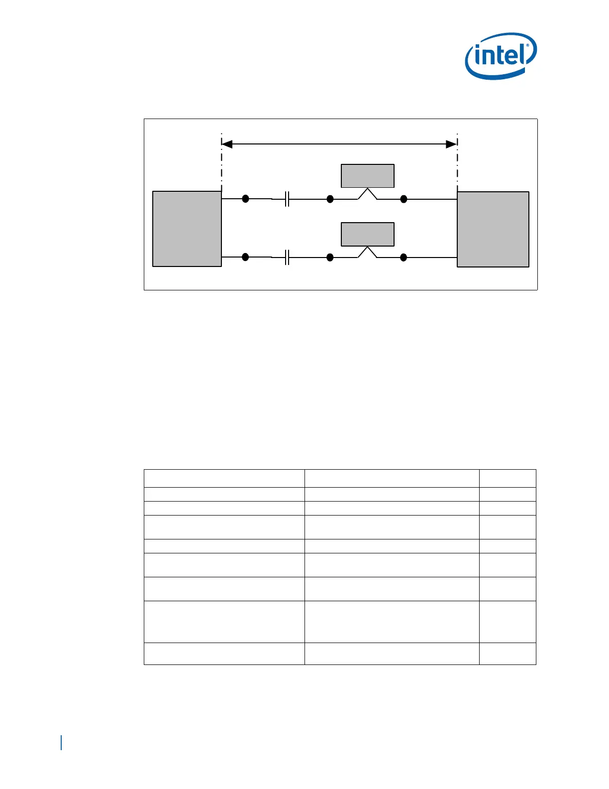
Table 52 and Figure 93 summarize the layout routing solution space to a PCI Express
connector. In this case, EP80579 is a receiver and the PCI Express connector is a
transmitter. LT must be routed on the same layer.
• L1 is the EP80579 breakout region.
• L2 starts from the EP80579 breakout region to the edge logic analyzer connector.
• L3 and L4 are the logic analyzer connector breakout regions on each side of the
connector.
• L5 is from the logic analyzer connector breakout region to the PCI Express
connector breakout region.
• LT is the main routing section that is from the EP80579 pin to the PCI Express
connector.
Figure 92. PCI Express Connector with LAI Connector Routing (EP80579 Transmit)
EP80579
PCI
Express*
Connector
L1
L2
AC CAP
LT = L1 + L2 + L3 + L4 + L5
LAI
Connector
L4L3 L5
L1'
L2'
AC CAP
LAI
Connector
L4'L3' L5'
Table 52. PCI Express Connector with LAI Connector Routing (EP80579 Receive) (Sheet
1 of 2)
Parameter Routing Guidelines Figure
Signal Group PEA0_Rn[7:0], PEA0_Rp[7:0] -
Reference Plane Ground Referenced -
Layer Assignment
Layers 3 or 8 (stripline)
Layers 1 or 10 (microstrip)
-
Characteristic Trace Impedance (Zo) 90 Ω ±10% (Differential) -
Nominal Trace Width
4.5 mils (stripline)
4.75 mils (microstrip)
Figure 87
Figure 88
Nominal Trace Spacing within a pair from
edge to edge
5.5 mils (stripline)
5.25 mils (microstrip)
Figure 87
Figure 88
Nominal Trace Spacing from edge of one
differential pair to edge of another
differential pair
The greater of:
• 18 mils or 3x dielectric thickness (stripline)
• 20 mils or 3x dielectric thickness
(microstrip)
Figure 87
Figure 88
Trace Length L1, L1’– EP80579 Breakout
region
Min = 0.5 in.
Max = 2.5 in.
Figure 93

 Loading...


