Intel
®
EP80579 Integrated Processor Product Line May 2010
Order Number: 320068-005US 336
System Memory Interface (Memory Down)—Intel
®
EP80579 Integrated Processor Product Line
B.4 DDR2 Signal Groups
Table B-24 summarizes the different signal groupings of the DDR interface. See the
Intel
®
EP80579 Integrated Processor Product Line Datasheet for more details on
specific pin functionality.
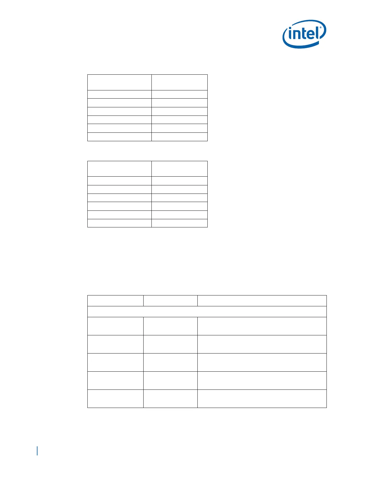
Table B-22. 1Gb Addressing
Configuration
DDR2
128 Mb x 8
# of Banks 8
Bank Address BA0-BA2
Auto Precharge A10
Row Address A0-A13
Column Address A0-A9
Page Size 1KB
Table B-23. 2Gb Addressing
Configuration
DDR2
256 Mb x 8
# of Banks 8
Bank Address BA0-BA2
Auto Precharge A10
Row Address A0-A14
Column Address A0-A9
Page Size 1KB
Table B-24. DDR2 Signal Groups (Sheet 1 of 2)
Group Signal Name Description
Data, Mask, & Strobe
Byte 0
DDR_DQ[0..7],
DDR_DM0, &
DDR_DQS0/DQS0#
Data Byte Lane0
Byte 1
DDR_DQ[8..15],
DDR_DM1, & DQS1/
DDR_DQS1#
Data Byte Lane1
Byte 2
DDR_DQ[16..23],
DDR_DM2, & DQS2/
DDR_DQS2#
Data Byte Lane2
Byte 3
DDR_DQ[24..31],
DDR_DM3, & DQS3/
DDR_DQS3#
Data Byte Lane3
Byte 4
DDR_DQ[32..39],
DDR_DM4, &
DDR_DQS4/DQS4#
Data Byte Lane4