Intel
®
EP80579 Integrated Processor Product Line May 2010
Order Number: 320068-005US 148
PCI Express* Interface—Intel
®
EP80579 Integrated Processor Product Line
10.1.10 Topology 4 – EP80579 to PCI Express Down Device
with Logic Analyzer Connector
Table 55 and Figure 96 summarize the layout routing solution space to a PCI Express
device on the board with a logic analyzer connector between the EP80579 and PCI
Express device. In this case, the EP80579 is a transmitter and the PCI Express device is
a receiver. All traces must be routed on the same layer.
• L1 starts from the EP80579 breakout region to the AC blocking capacitor via.
• L2 is the main routing section that is from the AC blocking capacitor via to the logic
analyzer connector.
• L3 and L4 are the logic analyzer connector breakout regions on each side of the
connector.
• L5 is from the logic analyzer connector breakout region to the PCI Express device
break-in region.
• L6 is the break-in region of the PCI Express device.
• LT is the main routing section that is from the EP80579 pin to the PCI Express
device.
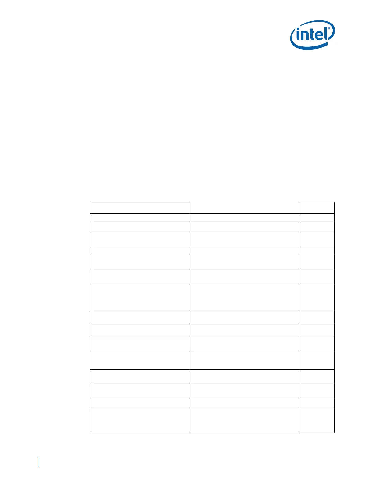
Table 55. PCI Express Down Device with LAI Connector Routing (EP80579 Transmit)
Parameter Routing Guidelines Figure
Signal Group PEA0_Tn[7:0], PEA0_Tp[7:0] -
Reference Plane Ground Referenced -
Layer Assignment
Layers 3 or 8 (stripline)
Layers 1 or 10 (microstrip)
-
Characteristic Trace Impedance (Zo) 90 Ω ±10% (Differential) -
Nominal Trace Width
4.5 mils (stripline)
4.75 mils (microstrip)
Figure 87
Figure 88
Nominal Trace Spacing within a pair from
edge to edge
5.5 mils (stripline)
5.25 mils (microstrip)
Figure 87
Figure 88
Nominal Trace Spacing from edge of one
differential pair to edge of another
differential pair
The greater of:
• 18 mils or 3x dielectric thickness (stripline)
• 20 mils or 3x dielectric thickness
(microstrip)
Figure 87
Figure 88
Trace Length L1, L1’– EP80579 Breakout
region and to AC CAP
Min = 0.5 in.
Max = 2.5 in.
Figure 96
Trace Length L2, L2’ – AC CAP to logic
analyzer breakout region.
Min = 0.5 in.
Max = 5.5 in.
Figure 96
Trace Length L3, L3’, L4, L4’ – Logic
analyzer breakout region.
0.5 in. (stripline) Figure 96
Trace Length L5, L5’ – Logic analyzer
breakout region to PCI Express device
breakout region.
Min = 2.5 in., Max = 6.5 in. Figure 96
Trace Length L6, L6’ – PCI Express
breakout region.
Min = 0.75 in.
Max = 2.0 in.
Figure 96
Trace Length LT– EP80579 pin to PCI
Express Device
LT = L1+L2+L3+L4+L5+L6 (stripline)
LT = L1+L2+L5+L6 (microstrip)
Figure 96
AC Blocking Capacitor–AC CAP 0.1 μF Figure 96
Length Tuning Requirements
Routing must remain on the same layer.
Maximum number of vias is 6 (stripline) and 4
(microstrip).
LT-LT’ = ±5 mils
Figure 96