Intel
®
EP80579 Integrated Processor Product Line May 2010
Order Number: 320068-005US 200
Synchronous Peripheral Interface (SPI)—Intel
®
EP80579 Integrated Processor Product Line
16.2.1 SPI Routing Guidelines
16.2.2 Boot BIOS Selection
GPIO[17] and GPIO[33] have internal 50 KΩ pull-ups which set the default bootup to
the FWH. The SPI boot option is implemented by strapping GPIO[17] and GPIO[33] to
ground (GND) through 1KΩ pull-down resistors. See Table 74 for strapping options.
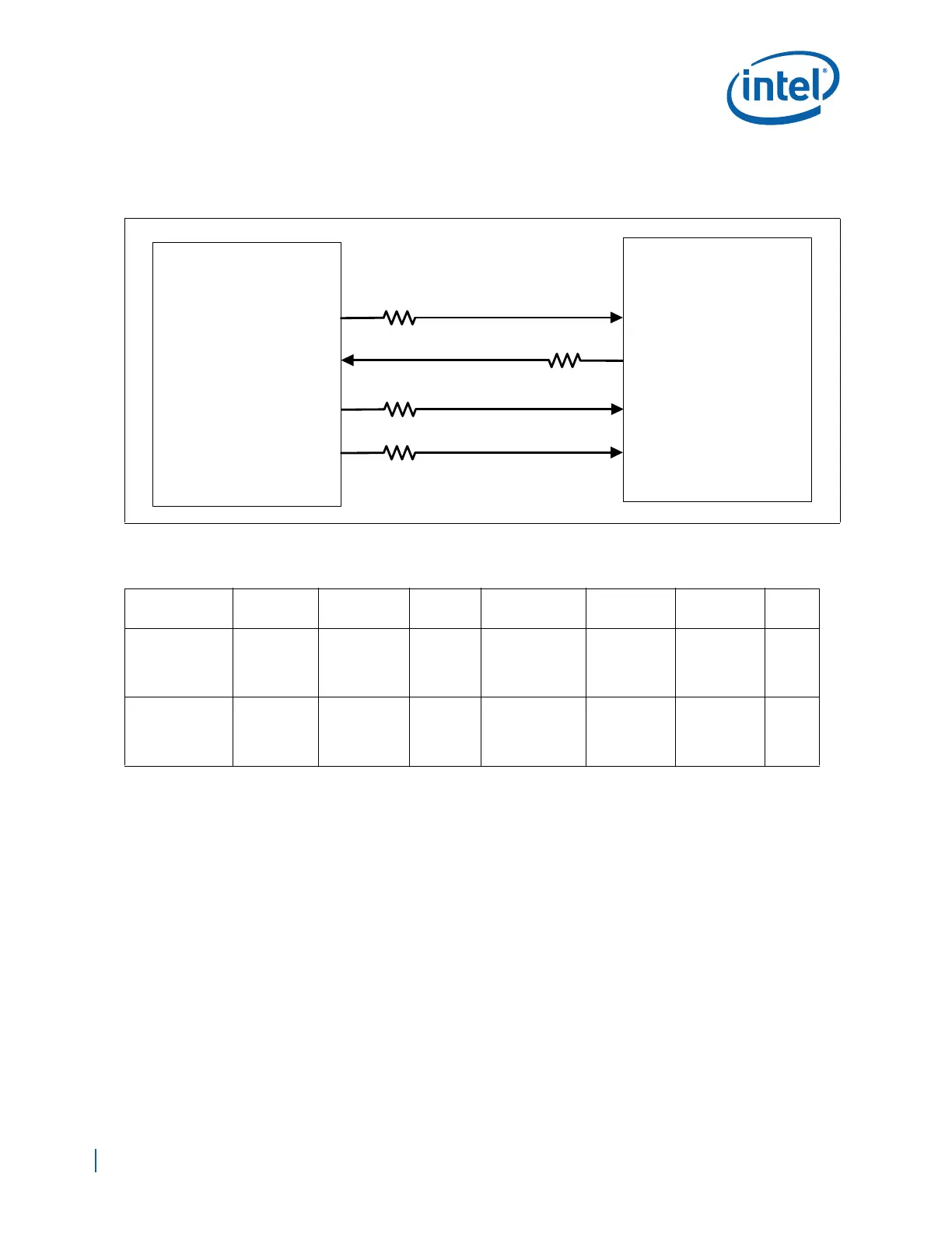
Figure 133. SPI Topology (System BIOS Only)
Table 73. SPI Single Flash Device Routing Summary
Signal Name Impedance
Width (W) /
Spacing (S)
Layer Length Breakout Figure Notes
SPI_MOSI
SPI_MISO
SPI_CS0#
SPI_CLK
50Ω ±10%
W = 4.5 mils
S = 7 mils
Microstrip
L1 = 1”-11”
L2 = 0.1”-0.5”
L3 = 0.1”-0.5”
W = 4 mils
S = 4 mils
L = <1”
Figure 133
1
,
2
,
3
1. W represents width of signal; S represents spacing to any other signal.
2. R1 = 15Ω and should be placed 0.1-1” from the EP80579.
3. R2 = 15Ω and should be placed 0.1-1” from the serial flash device.
SPI_MOSI
SPI_MISO
SPI_CS0#
SPI_CLK
50Ω ±10%
W = 3.75mils
S = 7 mils
Stripline
L1 = 1”-11”
L2 = 0.1”-0.5”
L3 = 0.1”-0.5”
W = 4 mils
S = 4 mils
L = <1”
Figure 133 1,2,3
EP80579
Serial Flash
Serial In
Serial Out
Chip Select
Clock
SPI_MOSI
SPI_MOSO
SPI_CS0#
SPI_CLK
R1
L2
R1
R1
R2
L2
L2
L1
L1
L1
L1
L3