Intel
®
EP80579 Integrated Processor Product Line—System Memory Interface (DIMM)
Intel
®
EP80579 Integrated Processor Product Line
Platform Design Guide May 2010
119 Order Number: 320068-005US
9.5 Package Length Compensation
Package length compensation is required for total routing length requirements, see the
length matching rules listed in Table 38. See the DDR2 Package length information in
the Intel
®
EP80579 Integrated Processor Product Line Datasheet for more information.
9.6 Length Matching and Length Formulas
The routing guidelines presented in the following subsections define the recommended
routing topologies, trace width, spacing geometries, and absolute minimum and
maximum routed lengths for each signal group. These guidelines are recommended to
achieve optimal signal integrity and timing.
9.7 DDR2 Interface System Interconnect
Figure 75 provides a block diagram of the system interconnect between the EP80579
DDR2 Memory Controller and the two DIMMs for the signal groups provided in Table 37.
The Command/Address and Control signals require external terminations. External
terminations are not required for DQ and DQS signals since both the EP80579 and the
SDRAMs contain internal ODT. The following sections provide the detailed topology and
routing guidelines for each of the signal groups.
DC Bias (I/O)
DDR_CRES[2:0]
• DDR_CRES[2:1] - Impedance compensation resistors.
• DDR_CRES[0] - Common return for DDR2 interface
compensation resistors on DDV_CRES,
DDR_SLWCRES and DDR_RCOMPX
DDR_SLWCRES Slew rate compensation for DDR2 interface (Analog)
DDR_RCOMPX Impedance compensation for DDR2 interface
DDV_CRES DDR2 resistor
DDR_VREF Voltage Reference (Analog)
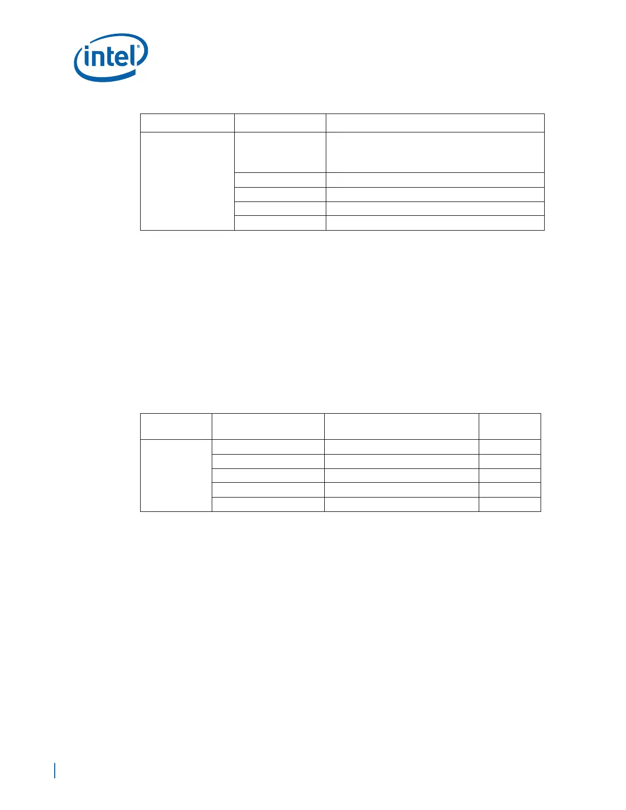
Table 37. DDR2 Signal Groups (Sheet 2 of 2)
Group Signal Name Description
Table 38. Length Matching Formulas between EP80579 and DDR2 DIMM
Source/
Destination
Signal Group to matching
signal
Total Length Matching Tolerances Comments
EP80579 Pad to
DDR2 DIMM
DQS to DQ/DM DQS = DQ/DM + 400 mils 1, 2
DQS to clock DQS = CLK/CLK# ± 500 mils 2
CMD/ADD to Clock CMD/ADD = CLK/CLK# ± 20 mils 2
CTRL to CMD/ADD CTRL = CMD/ADD + 2.5 inches 2
Clock to Clock# CLK[x] = CLK[x]# ±10 mils 2
Notes:
1. Length matching is only required within each Byte lane. Signal length matching is not required
outside the Byte lane. For example, any signal within DQ [0:7] need not be length matched to DQS
[3].
2. Total length means - L
PKG
+ L
BREAK
+ L
ROUTE