Intel
®
EP80579 Integrated Processor Product Line May 2010
Order Number: 320068-005US 340
System Memory Interface (Memory Down)—Intel
®
EP80579 Integrated Processor Product Line
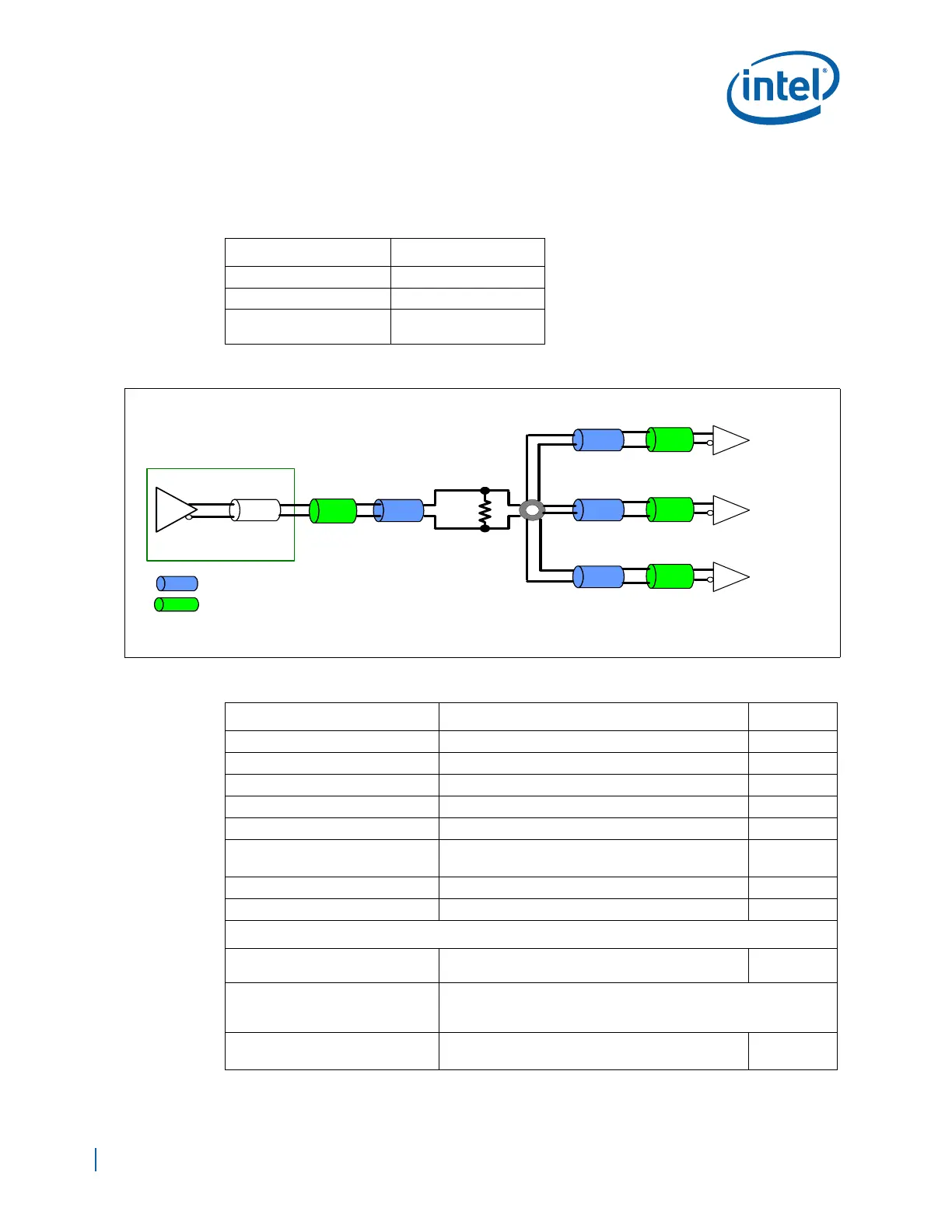
clock interconnect between the EP80579 and the memory devices. Table B-27 provides
the clock distribution among the memory devices, and Table B-28 provides the clock
routing guidelines.
Table B-27. Clock to Memory Device Mapping
Signal Connection To
CLK[0], CLK[0]# SDRAM[2:0]
CLK[1], CLK[1]# SDRAM[5:3]
CLK[2], CLK[2]#
SDRAM[7:6] +
ECC_SDRAM
Figure B-9. DDR2 Clock Signal Routing Topology (One Clock for Three Devices)
Table B-28. Clock Signal Group Routing Guidelines (Sheet 1 of 2)
Parameter Routing Guidelines Figure
Signal Group CLK[2:0]/CLK[2:0]#
Reference Plane Ground Referenced
Layer Assignment All clock signals must be routed on the same layer
Characteristic Trace Impedance (Zo) Single Ended Impedance: 45Ω ±10%
Nominal Trace Width See Stackup
Inter-pair Trace Spacing(e2e)
(CLK to CLK# spacing)
6.0 mils
Pair-to-Pair Spacing (e2e) 15.0 mils
Clearance from other signals groups 20.0 mils
Board Routing Guidelines
Total Trace Length (TTL) = (Lp + L0
+ L1 + L2 + L3)
Total Trace Length = 2.0 in - 5.0 in
Lp
Package Length:
See the Intel
®
EP80579 Integrated Processor Product Line Datasheet
for package length information.
L0
Microstrip Break-out
•Trace Length = 0.5in (max)
Pkg
EP80579
=
Stripline Routing
=
Microstrip Routing
SDRAM
Rtt
SDRAM
SDRAM
Lp
L1
L0
L0
L0
L3
L2
L0
L3
L2
L0
L3
L2
L0