Intel
®
EP80579 Integrated Processor Product Line—System Memory Interface (Memory Down)
Intel
®
EP80579 Integrated Processor Product Line
Platform Design Guide May 2010
341 Order Number: 320068-005US
B.6.4 DDR2 Data Group Signals – DQ/DM/ECC/DQS/DQS#
The DDR2 Data Group consists of the following signals:
• Data - DQ[63:0]
• ECC - ECC[7:0]
• Data Mask - DM[8:0]
• Data Strobe - DQS/DQS#[8:0]
The Data/DM and Strobe topologies shown in Figure B-10 and Figure B-11 are the
same for each Data Byte Lane (see Table B-24). All signals in the same data byte lane
should be routed on the same layer. The Data Strobe (DQS/DQS#) signals must be
routed as differential pairs with inter-pair skew of ± 6 mils. This topology assumes that
ODT is enabled for both the controller and SDRAM during write operations. Set
Controller ODT = 120 ohms, and SDRAM ODT = 150 ohms.
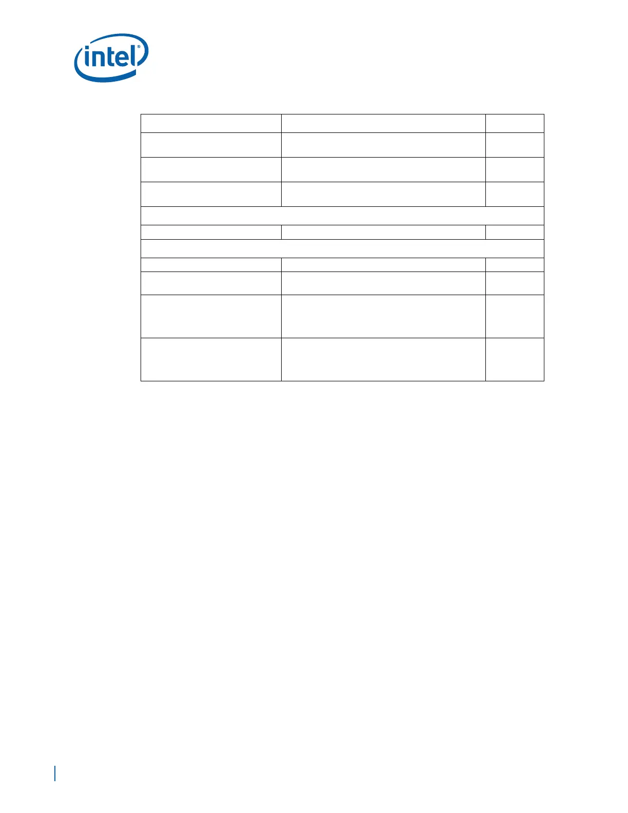
L1
Stripline Board Route
• Trace Length = 1.5 in (min) - 4.0 in (max)
L2
Stripline Board Route
• Trace Length = 0.8 in (max)
L3
Microstrip Board Route
• Trace Length = 0.5 in (max)
Resistor Coupling
Rtt 120 Ω ±1%
Routing Length Matching Rules
CLK-to-CLK# Length Matching Match clock pairs to within 10 mils
Pair-to-Pair Length Matching
Clock pairs should be matched in length to other clock
pairs within 20 mils of each other
Clock-to-DQS Length Matching
Match total length of DQS to clocks to within
±500 mils
• DQS/DQS# minimum Length = Clock - 500 mils
DQS/DQS# maximum Length = Clock + 500 mils
Clock-to-ADDR/CMD/CTRL
Match total length of ADD/CMD/CTRL to Clocks to
within 20 mils
• ADD/CMD/CTRL minimum Length = Clock - 0 mils
ADD/CMD/CTRL maximum Length = Clock + 20 mils
Table B-28. Clock Signal Group Routing Guidelines (Sheet 2 of 2)
Parameter Routing Guidelines Figure
 Loading...


