Intel
®
EP80579 Integrated Processor Product Line May 2010
Order Number: 320068-005US 118
System Memory Interface (DIMM)—Intel
®
EP80579 Integrated Processor Product Line
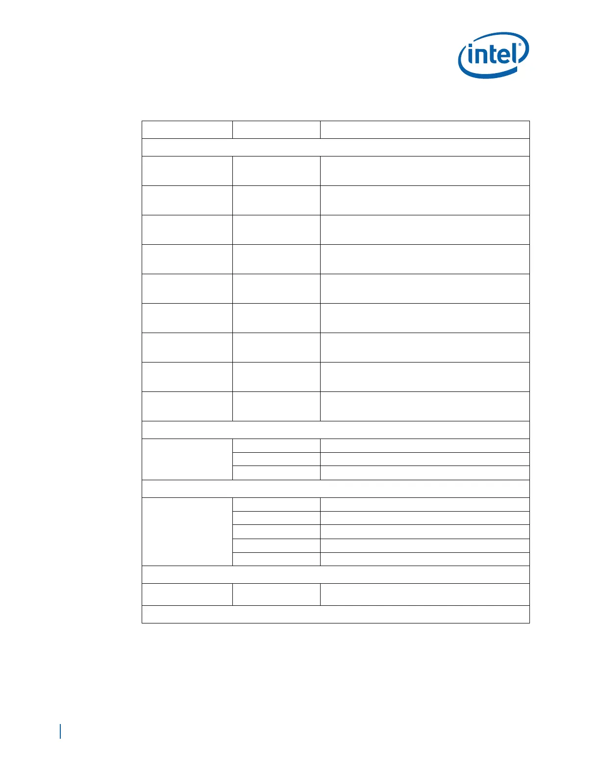
Table 37. DDR2 Signal Groups (Sheet 1 of 2)
Group Signal Name Description
Data, Mask, & Strobe
Byte 0
DDR_DQ[0..7],
DDR_DM0, &
DDR_DQS0/DQS0#
Data Byte Lane0
Byte 1
DDR_DQ[8..15],
DDR_DM1, & DQS1/
DDR_DQS1#
Data Byte Lane1
Byte 2
DDR_DQ[16..23],
DDR_DM2, & DQS2/
DDR_DQS2#
Data Byte Lane2
Byte 3
DDR_DQ[24..31],
DDR_DM3, & DQS3/
DDR_DQS3#
Data Byte Lane3
Byte 4
DDR_DQ[32..39],
DDR_DM4, &
DDR_DQS4/DQS4#
Data Byte Lane4
Byte 5
DDR_DQ[40..47],
DDR_DM5, &
DDR_DQS5/DQS5#
Data Byte Lane5
Byte 6
DDR_DQ[48..55],
DDR_DM6, &
DDR_DQS6/DQS6#
Data Byte Lane6
Byte 7
DDR_DQ[56..63],
DDR_DM7, &
DDR_DQS7/DQS7#
Data Byte Lane7
Byte 8
DDR_ECC[0..7],
DDR_DM8,
DDR_DQS8/DQS8#
Data Byte Lane 8 (ECC Check Bits)
Control
Control
DDR_CKE[1:0] Clock Enables - One per DIMM Rank
DDR_CS#[1:0] Chip Selects – One per DIMM Rank
DDR_ODT[1:0] On-Die-Termination – One per DIMM Rank
Address & Command
Address / Command
DDR_MA[14:0] Memory Address
DDR_BA[2:0] Bank Address (Bank Select)
DDR_RAS# Row Address Select
DDR_CAS# Column Address Select
DDR_WE# Write Enable (Output)
Clocks
Clocks
DDR_CLK[5:0]/
DDR_CLK#[5:0]
Differential Clocks – Three pairs per DIMM
DC Bias

 Loading...


