Intel
®
EP80579 Integrated Processor Product Line—Local Expansion Bus (LEB) Interface
Intel
®
EP80579 Integrated Processor Product Line
Platform Design Guide May 2010
243 Order Number: 320068-005US
One easy way to check this is to look at the specification of the device being used in the
design and look for the hold time on data during reads. In many occasions you will see
a few nanoseconds for Thold, but in some other cases the Thold = 0 nSec. This is the
case in which it is required to do something externally to meet this timing. A simple
solution that will resolve the hold time requirement would be to delay the EX_RD#
signal with a chip multilayer delay line. The Development Board design uses LDH32
2.5 nSec delay line to meet the EP80579 requirement of Trdhold=2nSec.
Note: By delaying the EX_RD#, you also must ensure that the Trdsetup still is valid. Normally
this is not a problem since the data becomes valid and is available early in time to allow
the to met setup.
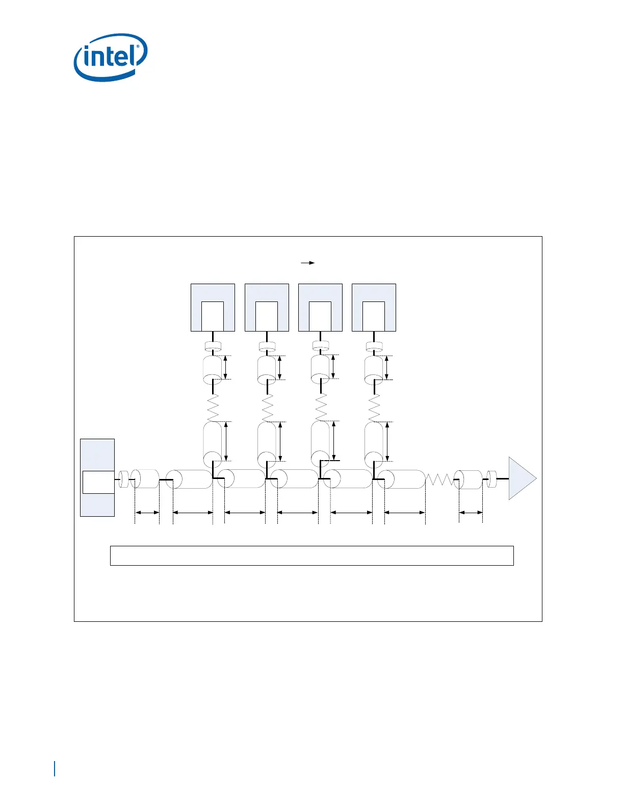
Figure 149. Data, and Control Signals Star Topology Diagram
Via Break out Break in
DATA
CNTL
BUFFER
EP80579
LDC_Brk_out LDC_TL1_route LDC_Brk_in
LDC_Brk_out + LDC_TL1_route + LDC_Brk_inLDC_Total =
NOTE: Breakout\ Breakin descriptions are as follows:
1. Routing where trace is 4 mil wide and 4mil spacing is implemented to escape\ enter BGA
2. The Breakout \ Breakin Length is defined from the pin of the BGA, to where 4 mil spacing
increases to the required spacing per SI recommendations.
a). CS = 10 mil edge-to-edge (e2e) for Stripline
b). CS = 12 mil edge-to-edge (e2e) for Microstrip
Via
Data and Control Star Topology
(EP80579 Peripheral)
TL1
LDC_TL3_route
TL3
TL2
TL2 TL2
TL2
Break in
LDC_Brk_in
DATA
CNTL
Via
TL3
Break in
LDC_Brk_in
DATA
CNTL
Via
TL3
Break in
LDC_Brk_in
DATA
CNTL
Via
TL3
Break in
LDC_Brk_in
DATA
CNTL
Via
LDC_TL2_route LDC_TL2_route LDC_TL2_route LDC_TL2_route
LDC_TL3_route
LDC_TL3_route
LDC_TL3_route
FPGA
STRATA
FLASH #1
COMPACT
FLASH
STRATA
FLASH #2
4XLDC_TL2_route +
DATA
CNRL
22 ohm 1%
22 ohm 1%
22 ohm 1%
22 ohm 1%
22 ohm 1%