Intel
®
EP80579 Integrated Processor Product Line—Platform System Clock
Intel
®
EP80579 Integrated Processor Product Line
Platform Design Guide May 2010
99 Order Number: 320068-005US
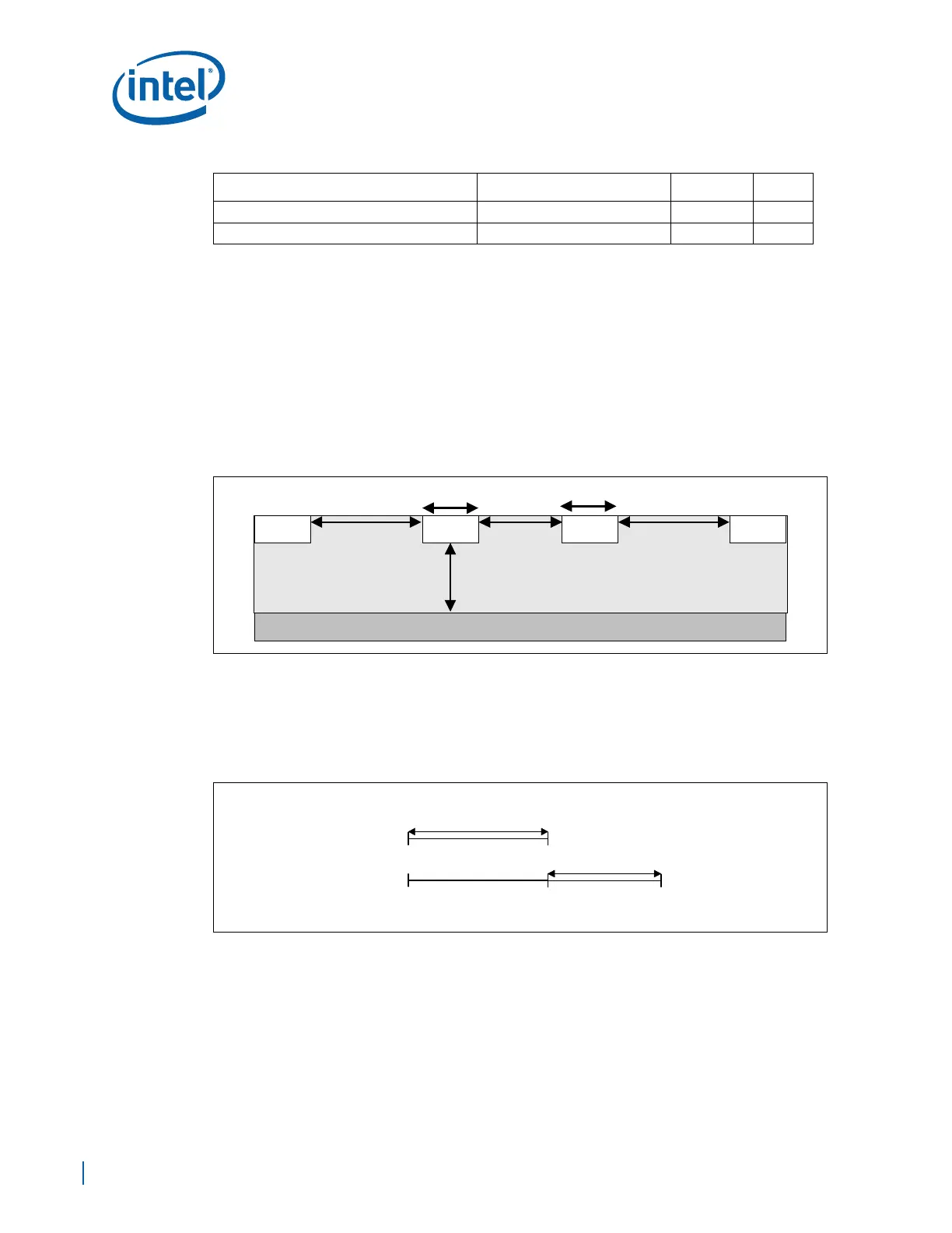
8.2.3 CLK33 Group
The driver in the CLK33 (PCICLK) group is the clock synthesizer 33 MHz clock output
buffer, and the receiver is the 33 MHz clock input buffer to the EP80579, LPC Clock,
Port80, Firmware Hub, TPM, and SIO.
Notes:
1. The 33 MHz clock to the EP80579 length, “Z”, can be 2” to 20” long and will dictate the length of all
other 33 MHz clock signals.
2. Figure 58 will be referenced in all subsequent 33 MHz clock routing sections.
Rs Series Termination Value 33 Ω ±5% Figure 56
Rt Shunt Termination Value 49.9 Ω ±1% Figure 56
Notes:
1. Routing guidelines are for the width is 4.5 mils with 10 mil spacing on layers 3 & 8. Use 4.5-mil line
width and adjust the trace to trace air gap to achieve 100 Ω differential impedance.
2. Clock traces are routed in a differential configuration. Maintain the minimum recommended
spacing between the two traces of the pair. Maintain uniform spacing along the entire length of the
trace. Do not exceed the maximum trace spacing, as this will degrade the noise rejection of the
network.
3. The differential impedance of each clock pair is the critical parameter. Single-ended impedance
may vary with different geometries.
4. Minimize L1, L2 and L3 lengths. Long lengths on L2 and L3 degrade effectiveness of source
termination and contribute to ringback.
5. Single Ended (SE) Absolute Vmax/Vmin (Includes overshoot/undershoot) specs of the transceiver
clock (CK410/DB800) 1.15v/-0.3v for some cases (means when the buffer is fast/Max) and
differential edge rate Max spec of 4V/ns (receiver clk), the min length is required to 3”.
Figure 57. Trace Spacing for 100 MHz SRC Clocks
Table 20. 100 MHz SRC/SRC# Clock Routing Guidelines for PCI Express Slot/Component
Parameter Routing Guidelines Figure Notes
h
S
WW
S1S1
SRC SRC#
Ground Plane
Figure 58. 33 MHz Clock Relationships
Z
CLK_33 to
EP80579
Z+ 0" to 6.0"
CLK_33 to Down
Devices (LPC
Devices)