Intel
®
EP80579 Integrated Processor Product Line—High-Speed Design Concerns
Intel
®
EP80579 Integrated Processor Product Line
Platform Design Guide May 2010
58 Order Number: 320068-005US
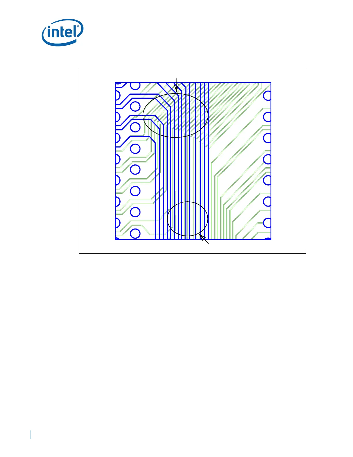
Figure 33. Signal Parallelism
Proper adjacent layer signal routing
Improper adjacent signal layer routing