Intel
®
EP80579 Integrated Processor Product Line May 2010
Order Number: 320068-005US 73
System Power Delivery Guide—Intel
®
EP80579 Integrated Processor Product Line
due to the transition or switching loss as it switches on and off. To minimize the
transition loss in the control MOSFET, its transition time must be minimized. This is
usually accomplished with the use of a small-size MOSFET. Or similarly, the duty cycle
of the Synchronous MOSFET is very large; hence, to minimize the DC loss of the
Synchronous MOSFET, its R
DS-ON
must be small. This is usually accomplished with the
use of a large-size MOSFET or several small-size MOSFETs connected in parallel.
However, this solution typically leads to shoot-through current as it is quite difficult to
minimize the effect of the Gate-Glitch phenomenon in the Synchronous MOSFET due to
the C
GD
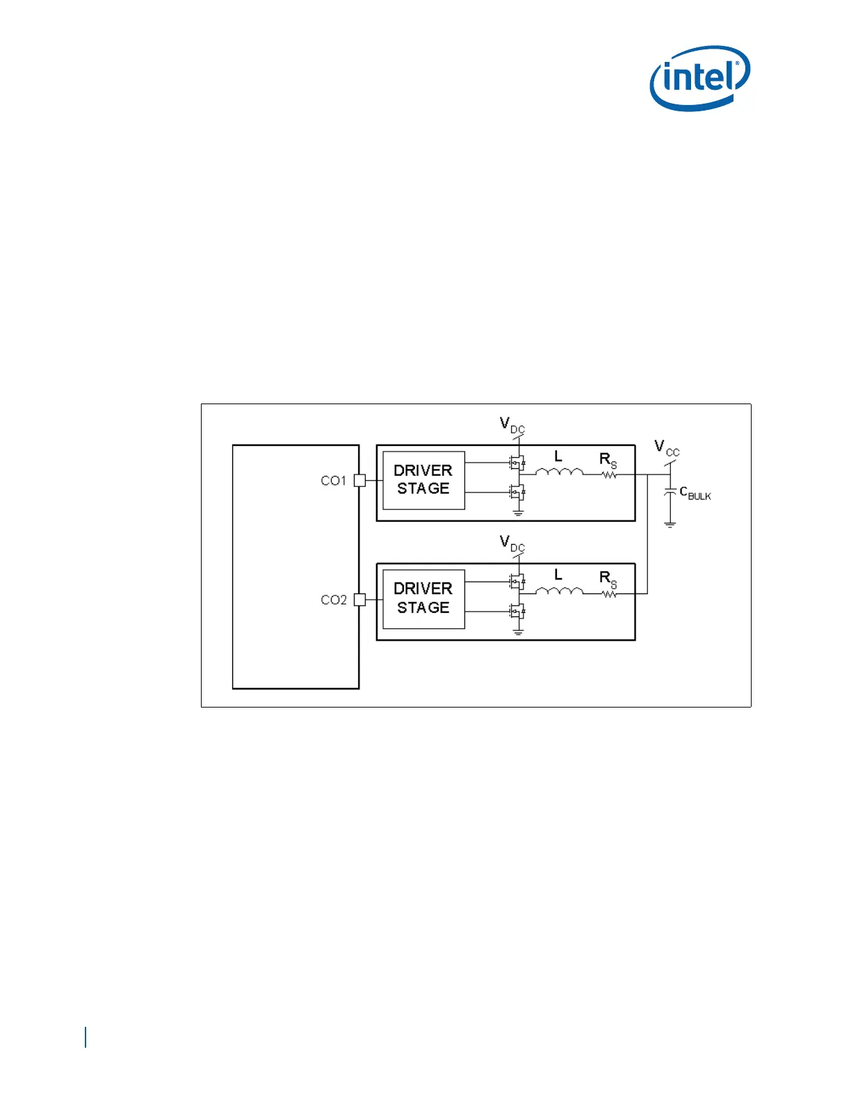
charge coupling effect. Therefore, it is necessary to go to a multi-phase
topology (Figure 40). In a multi-phase topology, the output load current is sourced
from multiple sources or output stages. The term multi-phase implies the phases or
stages are out of phase with respect to each other. For example, in a dual-phase
topology, the stages are exactly 180° output of phase.
Note: The Development Board implements only the single-phase topology for the switching
regulators. Where necessary, multiple MOSFETS are used to increase the output
current.
6.6.3 Voltage Regulator Design Recommendations
When laying out the processor power delivery circuit using a traditional Buck Voltage
Regulator on a printed circuit board, the example shown in Figure 41 must be followed.
Figure 40. Voltage Regulator Multi-Phase Topology Example