Intel
®
EP80579 Integrated Processor Product Line May 2010
Order Number: 320068-005US 171
Universal Serial Bus (USB) Interface—Intel
®
EP80579 Integrated Processor Product Line
12.3.2 GND Plane Splits, Voids, and Cut-Outs (Anti-Etch)
Avoid anti-etch on the GND plane.
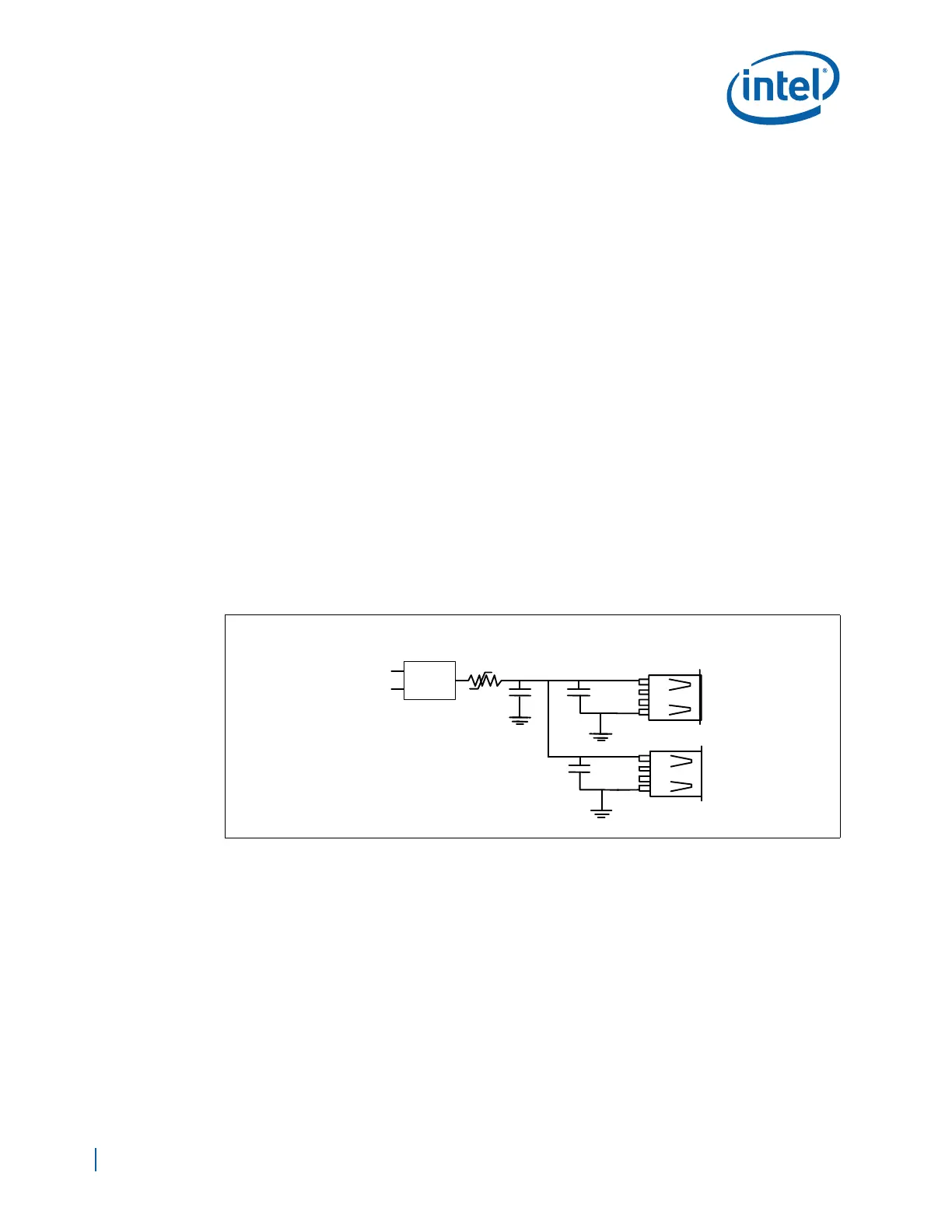
12.4 USB Power Line Layout Topology
The following is a suggested topology for power distribution of Vbus to USB ports.
Circuits of this kind provide two types of protection during dynamic attach and detach
situations on the bus:
• inrush current limiting (droop)
• dynamic detach flyback protection
These two different situations require both bulk capacitance (droop) and filtering
capacitance (for dynamic detach flyback voltage filtering). It is important to minimize
the inductance and resistance between the coupling capacitors and the USB ports.
Designers must place capacitors as close as possible to the port and the power-carrying
traces must be as wide as possible, preferably, a plane. A good general guideline is to
make the power-carrying traces wide enough that the system fuse will blow on an over
current event. If the system fuse is rated at 1 amp, the power-carrying traces must be
wide enough to carry at least 1.5 amps.
The USB power traces should be at least .050" wide to ensure adequate current
carrying capability. This requirement is implemented in the rule set by identifying USB
power nets and applying a minimum .050" line width to the entire net. Not all segments
of all of these nets will carry high current therefore the requirement built into the rule
set should be reconsidered as the design progresses.
12.5 EMI Considerations
The guidelines in the following sections apply to the selection and placement of
common mode chokes and ESD protection devices.
12.5.1 Common Mode Chokes
Testing has shown that common mode chokes can provide required noise attenuation.
A design must include a common mode choke footprint to provide a stuffing option in
the event the choke is needed to pass EMI testing. Figure 116 shows the schematic of a
typical common mode choke and ESD suppression components. Place the choke as
close as possible to the USB connector signal pins. In systems that route USB to a front
panel header, the choke must be placed on the front panel card. See Section 12.7.3,
“Front Panel Daughter Card” on page 176.
Figure 115. Good Downstream Power Connection
GGnndd
44
1
1
470 pF
μ
G
nndd
44
1
1
470 pF
V5REF 5 V
SWITCH
V5REFSUS

 Loading...


